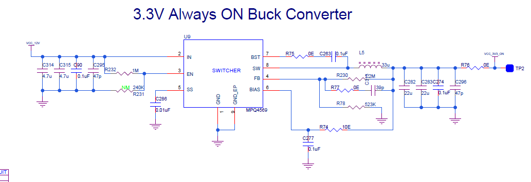
Hi Team, I would like to use the MPQ4569GN-AEC1 in our design. Our Vin(max)= 18V, Vin(min)=10.5, Vin(nom)=13.8, Vout=3.3V, Load current is 20mA. Kindly review it and let us know any feedback on the same.
Hello Abdul,
There appears to be nothing wrong with the way that you have your schematic. However, I have the following general notes:
- Ensure capacitors are 2-3x the voltage value they are subjected to in order to prevent any derating.
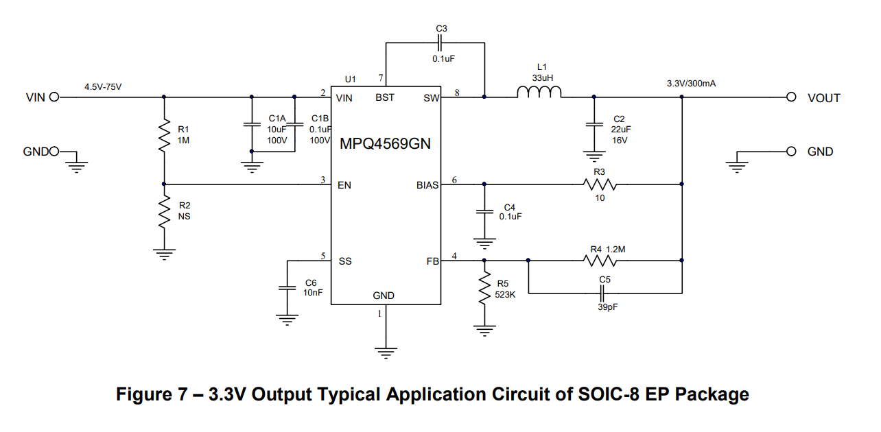
- If the capacitances you have limit the slew rate for any reason, shown below is a typical application schematic found in the MPQ4569 datasheet. This should give a good reference on values to be applied.
- From what it looks like, you followed the typical application quite well, so you should be good to go.
Please follow the following layout practices moving forward to mitigate any issues down the line:
- Keep the path of switching current short and minimize the loop area formed by input capacitor, high-side, low-side MOSFET and output capacitor.
- Bypass ceramic capacitors should be as close as possible to the VIN pin.
- Make sure that all feedback connections are short and direct. Place the feedback resistors as close to the chip as possible.
- Keep SW away from sensitive analog areas such as FB.
- For better thermal performance and long-term
reliability consideration, VIN, SW and GND should be connected to a large copper area respectively to cool the chip.
Please see the datasheet for any more details.
Best,
Krishan
Hi Krishnan,
In datasheet we not able to see any switching frequency range. Kindly confirm the max switching frequency range for this part.
Also we calculated for our current design please find it . please let us know any feedback on us.
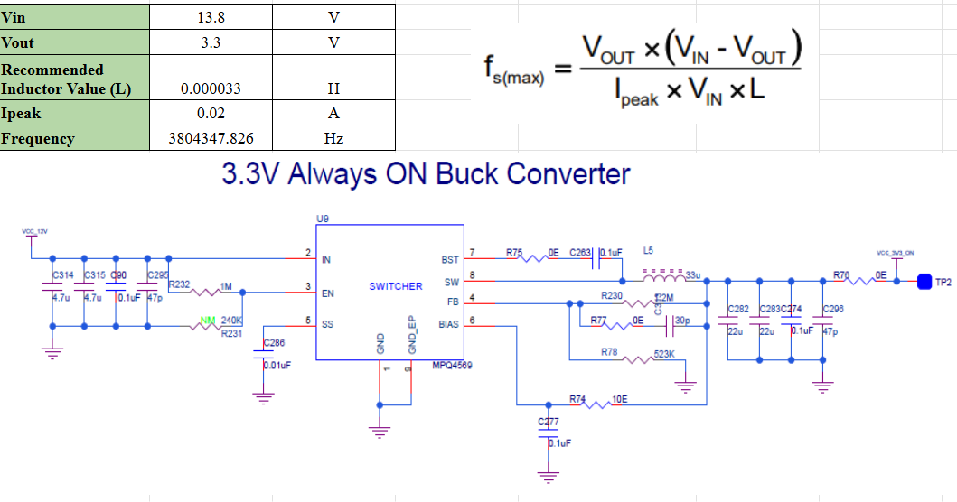
I see that your question has been answered in this post as this IC should not be operated above 1MHz.
Best,
Krishan Ram