Hello MPS team,
I am designing a product using the MA780GQ and I would like clarification on the recommended PCB treatment for the exposed pad and on bottom-side placement underneath the sensor.
From the MA780GQ datasheet, the package guidance says that the exposed pad should not be connected to GND or any other net, and that in general the device works well regardless of whether the exposed pad is connected, but if both options are possible it is recommended not to solder the exposed pad.
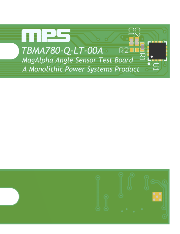
At the same time, when I look at the MA780 test board documentation, the evaluation hardware appears to use copper/vias under the MA780 device area, which makes the recommended implementation less clear from a production-design point of view.
I also found this MPS forum discussion, where an MPS engineer replied that it is OK to remove the pad from the footprint: Under chip pad treatment on MA780GQ-Z
Could you please clarify the following:
1- For a new production PCB design, is the preferred implementation to completely remove the exposed pad from the footprint?
2 -If the exposed pad is kept in the PCB footprint, should it always remain electrically floating and without solder paste?
3 -Is it acceptable to have copper and/or thermal vias in the PCB area underneath the MA780 package, as long as the exposed pad itself is not soldered to a net?
4 -Is it acceptable to place a component on the opposite side of the PCB directly underneath the MA780GQ?
5 -If bottom-side placement under the MA780GQ is allowed, are there any restrictions on:
- component type,
- copper density,
- keepout distance,
- magnetic/material restrictions,
- PCB thickness in that area?
My goal is to choose the safest layout approach for accuracy, manufacturability, and repeatability in volume production.
Thank you.