Hello,
I’m looking for assistance to better understand this design I’ve come across that was working but now isn’t. This is wound within a discontinued light stick from a Swedish home furnishing retailer, you know who I’m talking about, which I’ve liberated from its large tube exterior in an attempt to make it more streamline for an under counter kitchen workstation light. However somewhere between disassembly (de-soldering the light strip and input power wires) and reconstruction (soldering these back on once in new 3D printed enclosures) its stopped working, which lead me to understand the circuits design better, and thus here to ask “How did this even work in the first place?”
I’ve attached pictures to aid in the discussion:
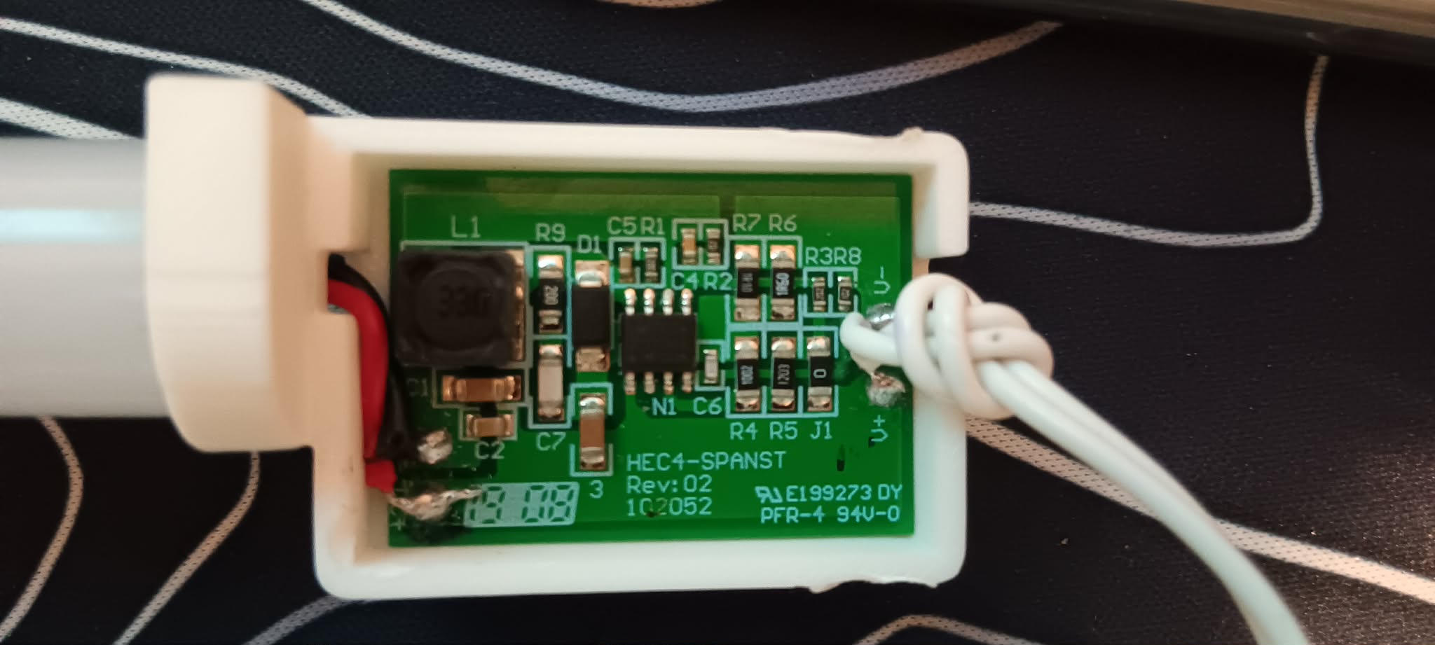
- The board with the USB 5V coming in on the right and the LED string output to the left.
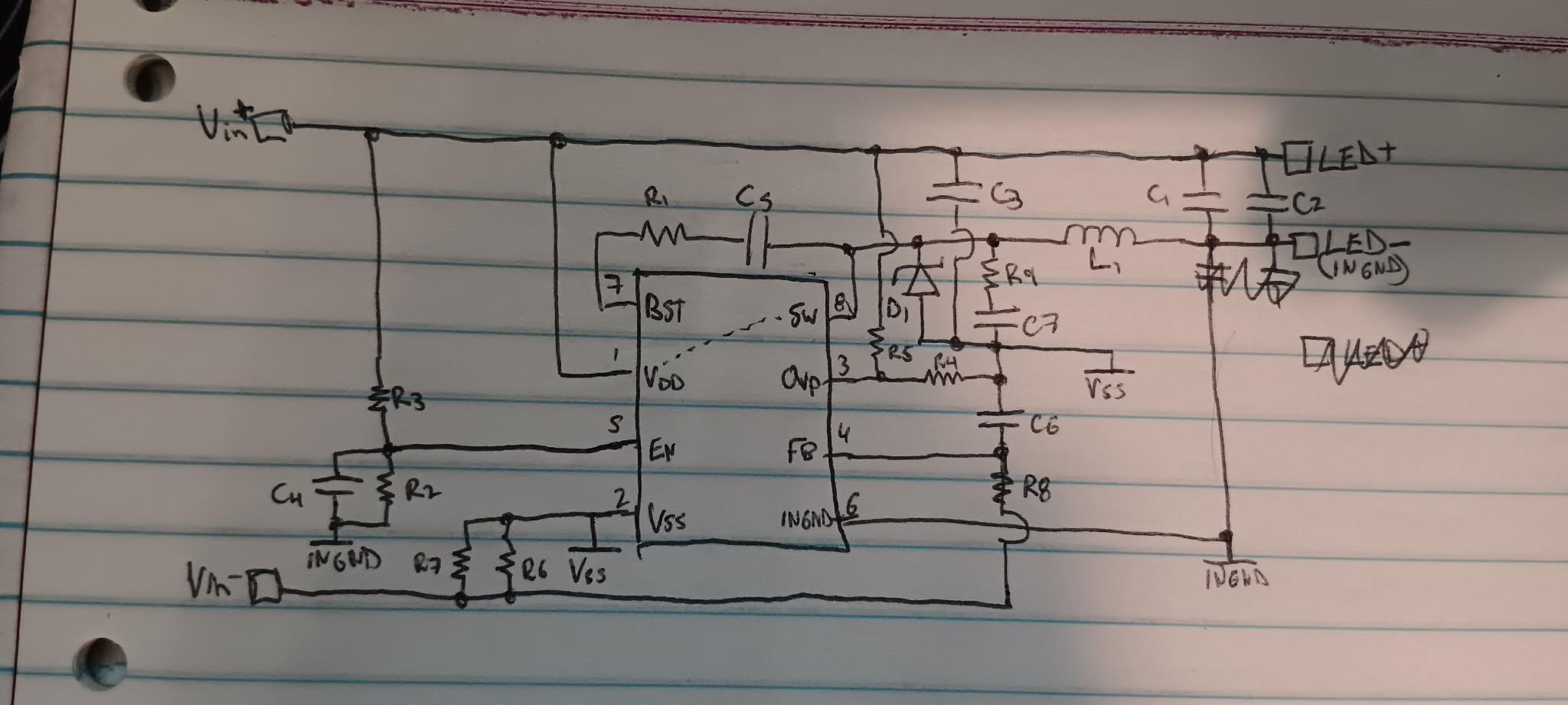
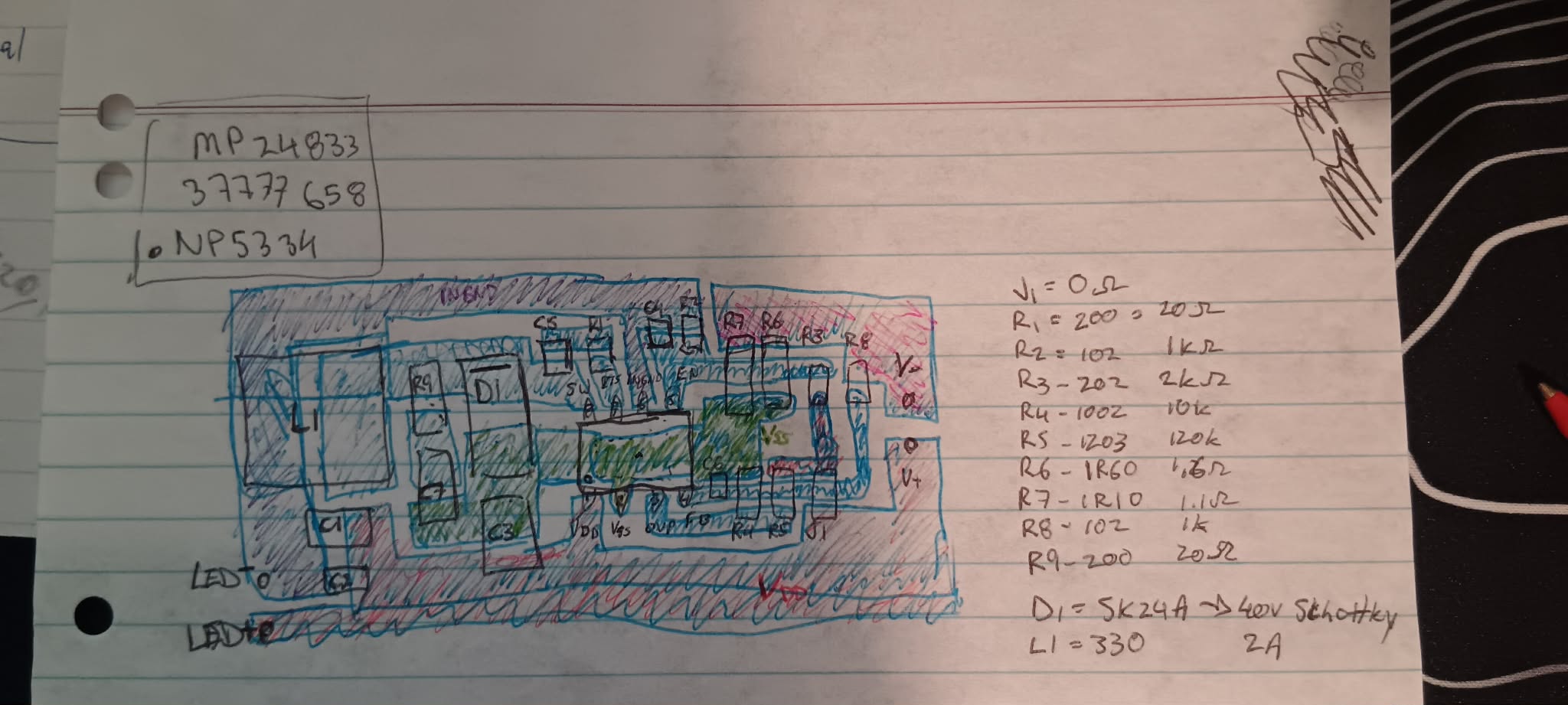
- My best attempt at a “Big Clive” board connections (particularly for tracks under the IC). Also noting the values of the resistors, diode and inductor; the caps don’t have markings to ID them.
- My understanding of the schematic, which I believe to be a set up ass a boost converter.
The LED string is 104 white LEDs in a 4s/26p configuration with each LED having Vf = 2.583V but the string as a whole having Vf = 2.13v (which doesn’t make sense to me)
My leading uncertainty is how the Enable pin (pin 5) is lifted to >1.35v with respect to INGND given there doesn’t seem to be any relation between INGND and Vin-. Measuring the voltage at the EN pin wrt INGND there is only 0.2V, which is not enough to turn on the chip, but somehow it was before.
Any assistance or suggestions on what may have been broken during the deconstruction and reconstruction and an explanation on how this circuit works would be greatly appreciated.
Thank you
My apologies, the orientation of L1 is Left-Right and there isn’t a connection across the top half of the board, that’s a drawing error.