Support Required – MP8017 PoE PD Output Voltage Issue (17V at No Load)

Hi Sir,

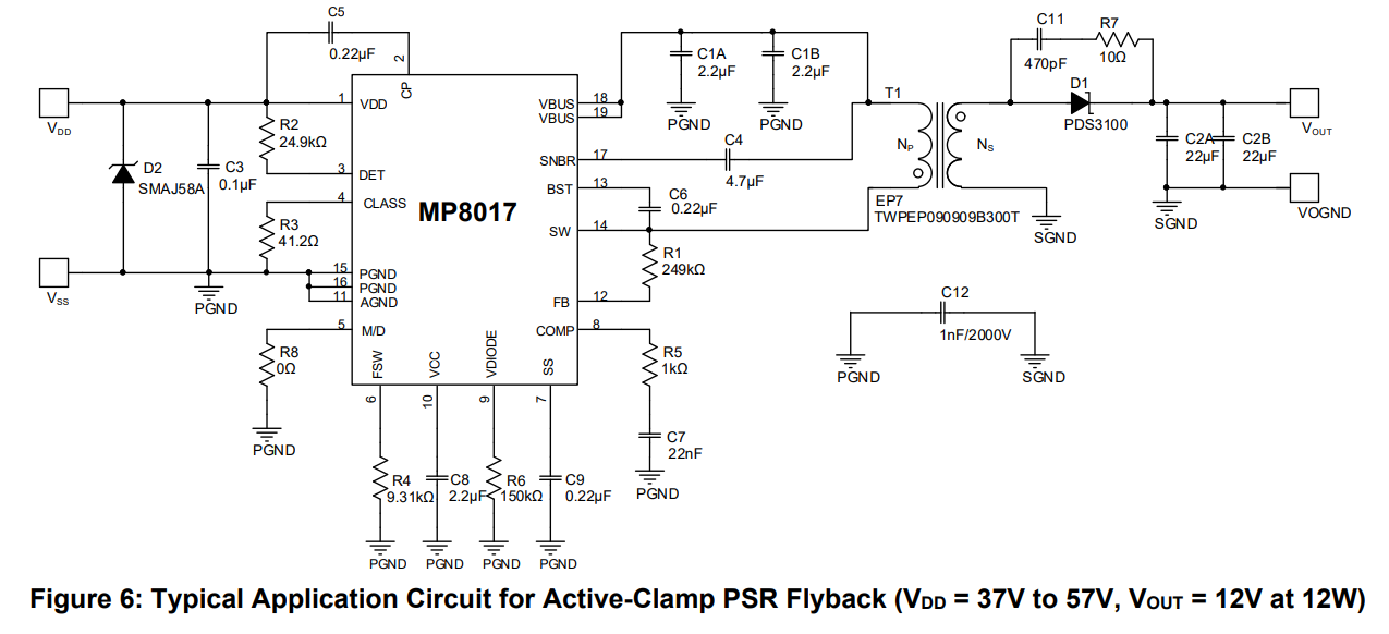
We have selected the MP8017 PD controller and designed a PoE-based power solution targeting a 12V output.

During testing, we applied power through a PoE injector and observed approximately 46V at the bridge rectifier input, which is within the expected range. We also provided an external VCC supply of 5.2V for proper startup.

However, we are currently observing an output voltage of around 17V under no-load conditions, whereas the design target is 12V.

We would like your support in understanding and resolving this issue. Specifically:

  • Is this behavior expected under no-load or light-load conditions?

  • Are there any recommended minimum load requirements for proper regulation?

  • Could you suggest any design improvements to achieve tighter output regulation?

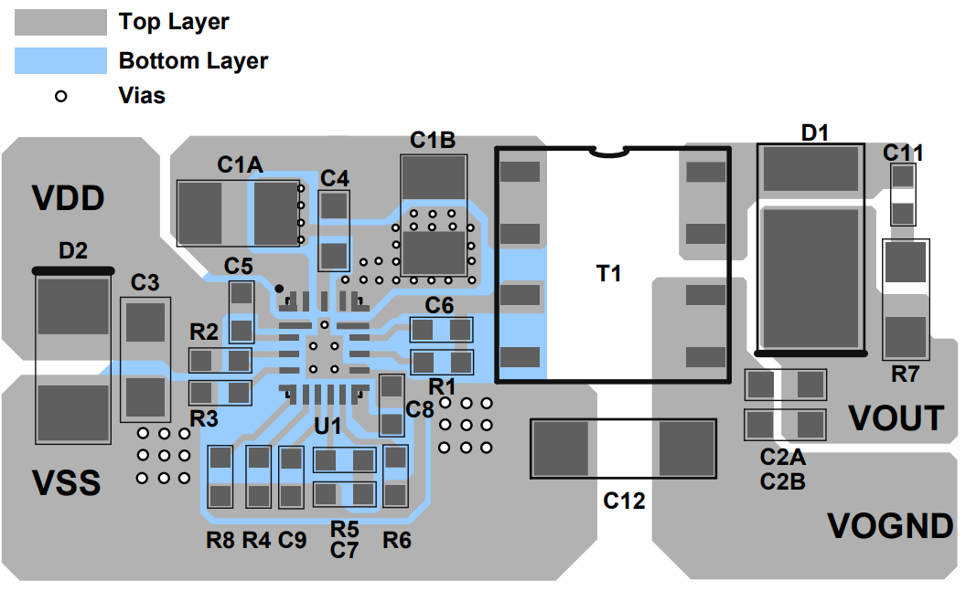
We have referred to the evaluation board design (EVL8017-L-00A) and request you to kindly share:

  • Detailed schematics (if available beyond the reference)

  • User guide / application notes for debugging

Due to tight project timelines, your prompt support would be highly appreciated.

Best regards,
Samudralankaia

Hello,

These are some good questions. For my understanding, how are you using the MP8017? Are you using a Primary Side Regulation (PSR) or Secondary Side Regulation (SSR) topology?

I can only assume since you designed your MP8017 from an EVL8017-L-00A, you are using a PSR Flyback topology. Generally, a SSR topology will have better regulation compared to a PSR topology.

For reference, here is the typical application schematic as shown in the datasheet. Does your schematic align with what you see here?

Here is the recommended layout for the MP8017 assuming this schematic above and PCB Layout guidelines for the following layout:

PCB Layout Guidelines:

Efficient layout of the PoE front-end and high-frequency switching power supply is critical for stable operation. A poor layout may result in reduced performance, excessive EMI, resistive loss, and system instability. For the best results, follow the guidelines below:

1. Keep the input switching loop between the flyback input capacitor, transformer, SW pin, and PGND as short as possible.

2. Keep the output loop between the rectifier diode, output capacitor, and transformer as short as possible.

3. Keep the active clamp loop between the active clamp capacitor, transformer, SW pin, and SNBR pin as short as possible.

4. Keep the input hot-swap loop between the PD input capacitor, VDD pin, VBUS pin, and VBUS capacitor as short as possible.

5. Place the VCC capacitor close to the VCC pin for optimal decoupling.

6. Ensure that the feedback trace is short and routed far away from noisy sources, such as SW.

7. Keep other signal leads (e.g. DET, CLASS, COMP, VDIODE, SS, and FSW) as short as possible.

8. Shorten the CP loop and BST loop for excellent hot-swap and HS-FET driver function.

9. Use a single-point connection between power GND and signal GND.

10. Place copper and vias under the MP8017 package for excellent thermal sinking.

Let me know if there are any more questions. To receive the layout files for the EVB for further reference, please submit a ticket using the following link: Contact MPS - Design Assistance Contact

Hi @Krishan.FAE ,
Recently I raised one query in forum page.
Can you please have a look at it?