Hi Harjit,
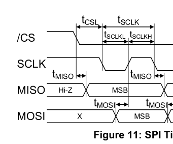
t(CSL) is just the minimum time between dropping CS and the beginning of the master clocking in data. So, for SPI mode 3, it would just be the min time between CS going active (low) and your first rising clock edge.
If that specification is not met, the result could be the MA missing your first SCLK transition and not seeing the first bit of data on MOSI or not transmitting over MISO until the next SCLK cycle.
Mode 0 is essentially the same as Mode 3 except that the SCLK is inverted. So, you can use the same timing diagram, just invert the clock signal. In the case of M0, t(CSL) must be held before we see the first rising edge after CS is asserted.
Would be great if this can be captured in all the MA* products with SPI. I must have read the different datasheets at least a dozen times and I missed it until the last time.