Hello ,
I refer reference design 48 V to 12V 15A , note of MPQ2908
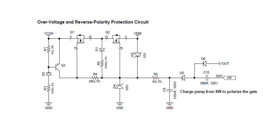
I cannot clearly understand working of Attached circuit.
I request for helping in understanding and explanation of this circuit.
Hello ,
I refer reference design 48 V to 12V 15A , note of MPQ2908
I cannot clearly understand working of Attached circuit.
I request for helping in understanding and explanation of this circuit.
Hello Piysuh,
Welcome to the MPS Forums!
I see you have looked at the MPQ2908 Reference Design. The two FETs connected between VCON and VEMI serve to protect against over-voltage or incorrect polarity connection at the input. Q1 provides controlled power path switching under normal operating conditions whereas Q2 mainly handles the reverse polarity protection.
Here is a basic outline of the functionality of this circuit:
Overall, under normal conditions, this circuit ensures smooth operation with minimal resistance while offering protection to the IC.
Hopefully this helped and offered some insight.
Best,
Krishan
It is lossy, with a drop of probably 4V until the SW starts switching and charge pumps the gates of Q1 and Q2 high. Prior to SW charge pumping the gate of Q2 is at Vcon minus the diode drop of Q1 which would put VEMI at a little more than a vth of Q2 lower than that, The Vout is clamped at less than 65V by diode D4 ( Vout will be a threshold lower than that.