Hello,
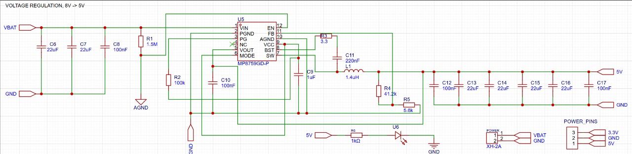
I’m using the MP8759 to step down 8V to 5V, and I followed the recommended application circuit from the datasheet. However, I’m running into some problems. Here’s what I’m seeing:
- Input voltage: 8V
- Output voltage: 2.6V (instead of 5V)
- Feedback voltage: 0.3V (should be 0.6V for proper regulation)
- PG pin: 0V
- Enable (EN) pin: 2.5V
- VCC pin: 3.51V
The feedback resistors I used are:
- R4=41.2kΩ (between VOUT and FB),
- R5=5.6kΩ (between FB and GND).
What’s strange is when I measure R4 in-circuit, it reads about 21kΩ, even though the actual resistor value is 41.2kΩ. This makes me wonder if there’s some internal resistance at the FB pin that’s causing the issue by effectively reducing R4 in parallel.
I’ve even replaced the MP8759 chip three times to rule out any issues with the IC itself, but the problem hasn’t gone away.
I’ve attached my schematic for reference. Could you please take a look and let me know what might be going wrong? Specifically:
- Is there any internal resistance at the FB pin that’s affecting the feedback network?
- If so, how can I work around it to get a stable 5V output?
Hello @fanuelpeter007,
Welcome to MPS forums. I see the desired operation is forced PWM mode since Mode pin is attached to VCC. What type of resistors are you using as feedback resistors? There might be resistors with high tolerance % which can lead to this difference at the output. Please use film resistor with 1% tolerance as feedback resistors.
Best,
Saquib
Hi @Saquib.FAE ,
Thank you for your response.
The feedback resistors I’m using are as follows:
- R4 : 100mW Thick Film Resistor, 75V, ±1%, ±100ppm/℃, 41.2kΩ
- R5 : 100mW Thick Film Resistor, 75V, ±1%, ±100ppm/℃, 5.6kΩ
Both resistors are rated at 1% tolerance, so I don’t think that is the problem
But could forced PWM mode potentially contribute to the reduced output voltage (2.6V)? Would switching to PFM mode help resolve this issue?
Hello @fanuelpeter007,
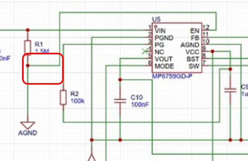
I also notice one thing is your schematic. The EN is connected to AGND. I believe this might be the root cause of this failure. Please double check the EN and GND connection and compare it with the DS.
Best,
Saquib
Hello @Saquib.FAE ,
I noticed this as well, but AGND is just a net name (connecting the 1.5MΩ resistor to the EN pin) and is only used in this specific instance. It is not functionally connected to GND anywhere else in the circuit.
To see if this was the problem, I replaced the 1.5MΩ resistor with a voltage divider to provide a stable 2.5V (the same voltage as with the 1.5MΩ resistor) to the EN pin. However, the issue persisted, and the output voltage remained low.
During troubleshooting, I observed that the in-circuit measurement of R4 (actual value 41.2kΩ) was reduced to ~21kΩ. To test further, I replaced R4 with a higher resistance (870kΩ) and R5 with 4kΩ. This brought the effective R4 in-circuit to ~42kΩ, which increased the output voltage to 3.5V.
Why does the effective resistance of R4 change so significantly in-circuit? Could this be due to an internal resistance at the FB pin? But also I noticed a buffer at the FB pin input in the DS
Hello @fanuelpeter007,
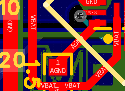
There might be a chance of a layout issue. In order to review your layout, you will have to submit a ticket and we will be able to review your layout.
MPS NOW Technical Support form
Best,
Saquib
Hello @fanuelpeter007,
Were you able to find the potential root cause of the issue?