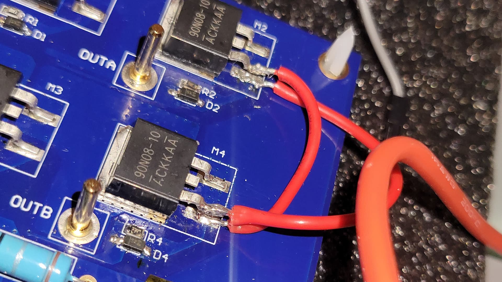
Before reconfiguring the board, I confirmed that the eval board was working without any rework. I lifted the gate pin of M2 and M4 and put a jumper wire between them to swap the gates and then I disabled ENB. So that GLA controls M4 and GLB controls M2. This is so that when I enable ENA M1 and M4 are both on and M3 and m2 are off. But unfortunately, I see a fault. I don’t have a load between SHA and SHB yet because I wanted to see if I could get it running without getting a fault. I’m not really sure why I am seeing a fault. Is it possible for the IC to work in the configuration I desire? If so, what changes do I need to make on the dev board to make it possible. Thanks
Can you share a picture of your rework or annotate the evaluation board schematic showing the changes?
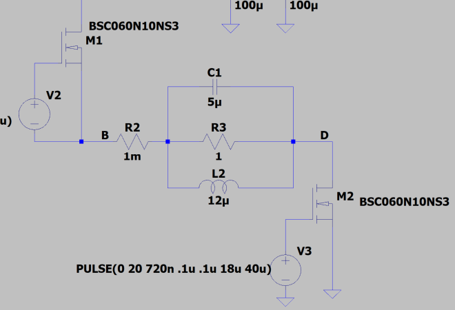
Can you clarify if that Spice schematic you uploaded is your current setup, or is it what you plan to do with the modified board?
Have you tested M1 and M4 individually to see if they work?
From the MP6528 block diagram, the following triggers nFAULT: TSD (thermal shutdown), UVLO, short-circuit (measured through VDS), and over-current (measured through low-side sense resistor). I have a feeling that short-circuit is being triggered due to floating switch node, so I recommend you try connecting a load between OUTA and OUTB (like an LC filter to simulate a buck), and then see if the FETs switch.
Here is a picture of the rework. I had already done it and tested it when I posted this question. The picture makes it look like there isn’t much of a gap between the pin and the pad but I assure you there’s a sufficient enough gap and there is not shorting between the pad and the lifted pin.
The spice model was to show that I only wanted to use 2 FETs in a half bridge configuration. Therefore, it is what I had planned to do with the modifed board.
Yes. Before, I did the rework I tested the circuit to see if works. M1 and M4 are working.
What do mean by floating switch node? is that SHA and SHB? My load is an inductor and resistor like in the spice model. I can try that.
Yes, I meant SHA and SHB. If you want to test the board without adding a load, you can try by completely disconnecting the gate terminals of M2 and M3 from the circuit, short the OUTA and OUTB headers, and then check if the fault condition is still existing.
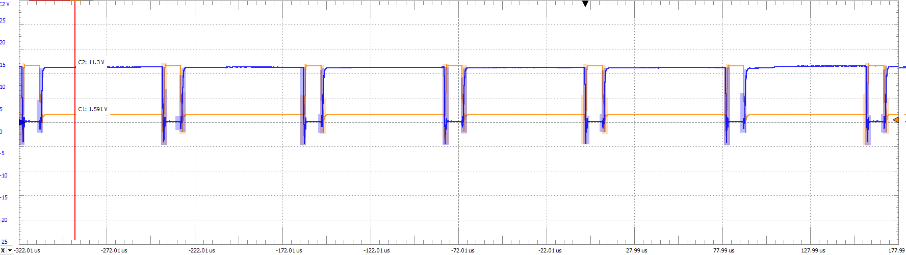
Hi, what worked for me was disconnecting the gates I wanted to use and pulling OC_REF up to VREG with a 100k resistor. This disabled the fault. Anytime there was a fault I would power cycle the device and it would output the pwm signal. However, something I am noticing is that the high and low gate outputs (GHA and GLA) are complementary pwm signals that are opposite in polarity. See screenshot of my scope below. Is there a way to get them to be the same polarity?
Apologies for the late reply; MPS had a company shutdown for the holidays. Yes, short circuit protection can be disabled by connecting a 100kΩ resistor from VREG to the OCREF pin, but I recommend to thoroughly test your system to rule out the possibility of short circuit in your system.
Regarding the gate outputs GHA and GLA, they are designed to operate in complementary signals. This is to prevent shoot-through of the same phase.