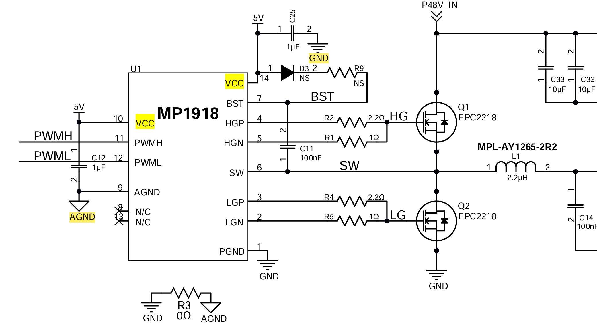
I would like to ask you about the ground and power supply connections for the MP1918 Gate Driver.
The datasheet states that AGND and PGND must be separated in the PCB layout to prevent noise from transferring from the PGND to the AGND, and a 0-ohm resistor should be connected between AGND and PGND.
My questions are:
-
Why is it necessary to connect AGND and PGND via a 0-ohm resistor?
-
Am I forced to connect this resistor between them, or can I just leave the grounds completely separated?
-
Why is there a separation of these grounds inside the IC in the first place?
-
If I connect the PWM inputs (which are referenced to AGND) to an Isolator chip that outputs PWM signals referenced to PGND, does this mean I cannot use an isolator at all with the MP1918?
-
Regarding the VCC connection: the component has VCC1 (pin 14) which must be referenced to AGND, and VCC2 (pin 10) which is referenced to PGND. If I connect both VCC1 and VCC2 to the same 5V source, but on the board one is referenced to PGND and the other to AGND, noise will enter the 5V line and pass into the VCC1 supply. If so, what is the benefit of connecting VCC this way?
Hello, I will answer your questions in the order asked.
-
What you said about AGND and PGND being separated in the PCB layout to prevent noise from transferring from the PGND to the AGND is true. But we want to ensure that AGND and PGND are at the same voltage potential, hence the 0Ω resistor.
-
If you left the AGND and PGND planes completely separated, that would mean that both GND planes run the risk of operating at two different potentials. From a controls standpoint, AGND and PGND have to be at the same voltage potential.
-
Like what the datasheet said, these GND planes prevent noise from transferring from the PGND to the AGND. As the signals involved in AGND are small and more sensitive and PGND can be subjected to switching noise from power components, the planes are mostly separated.
-
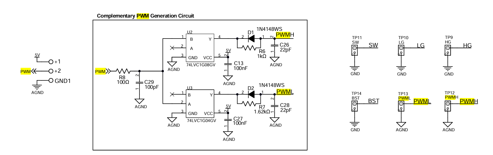
The PWM Generation Circuitry are all referenced to AGND. This should be reflected in your application as shown:
5. Usually, we would see VCC exclusively being connected to AGND. However, I can see it is specified in the layout guidelines in the reference schematic that they should be connected to both AGND and PGND.
After looking at the applications in which VCC is connected, this makes some sense:
VCC is being used to supply a reference to the BST loop, which is a part of the power loop. Connecting to AGND from this point would surely inject noise to AGND and other analog signals. It is decoupled to AGND in another area as well to further match the potential.
Best,
Krishan