In the MP5515 datasheet, the PFI pin is defined as open-drain, but PGB and PGS are not. Interestingly, the Electrical Characteristics table treats PGB and PGS as if they are open-drain outputs. If these pins are standard CMOS outputs, the V_OH and V_OL levels should be specified, yet they are absent from the table. Could you clarify the output structure of the PGB and PGS pins?
Hi Murphy,
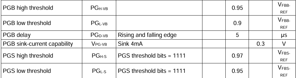
The PGB and PGS are not open-drain. The high and low threshold can be found in the EC table under PGB and PGS threshold:
Thanks,
George
Thank you for your reply, george.
However, the table above lacks the output voltage specifications for the PGB and PGS pins.
If these pins are CMOS outputs, the V_OH and V_OL specifications must be present.
If these pins have internal pull-ups in the MP5515, I would like to know the values of the pull-up resistors and the voltage source to which they are pulled up.
The thresholds in the table appear to be the reference voltage settings for the comparator that determine whether the PGB and PGS pins are high or low.
Also, the “sink-current capability” in the table is typically found in open-drain output specifications.
Please verify this once again.
Thank you.