Hi everyone!
I have a question while I am reading an application note.
The detailed link of this application note is mentioned under this writing.
I do not understand in detail while I am referring under two sentences.
One sentence said that it would be better to design the distance between components minimally.
The other sentence said that it would be better design the distance as possible as far away.
What is the difference meaning between two sentences ?
“Therefore, a certain minimum distance is required between the noise source, filter components, and connector”
“To avoid directly coupling the E- and H-fields of the DC/DC converter into connectors and cables, the circuit must be placed as far from the PCB connection points as possible”
link
Hi jh0507.cho,
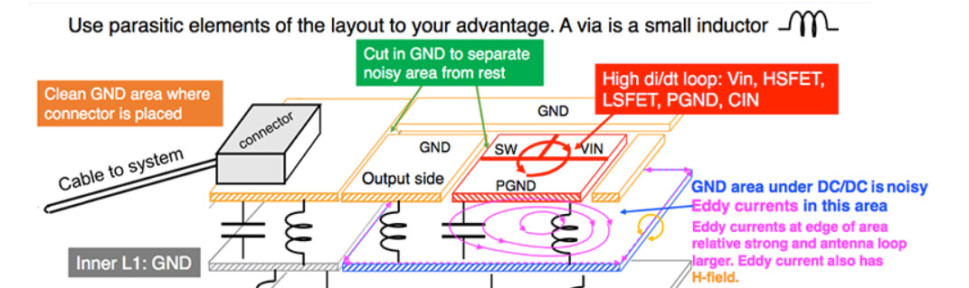
The first sentences is referring to a general rule of thumb to keep in mind when designing for Low EMI DC/DC converters. The filter circuit and control signal circuitry need to be in close proximity, implying on same plane on the PCB. Trace width for PCB traces connecting signal and power components need to be considered during the design.
On the PCB, the components are distributed between power plane and signal plane to minimize the effects of noise.
Regarding the second sentence, we want the connector to be far away to avoid coupling.
Attaching image from Fig 2 of article to help illustrate what I have described.
Regards,
Nouman
1 Like
Thank you for replying my question.
The first sentence is mentioned like that “a certain minimum distance is required between the noise source, filter components, and connector”.
In the upper sentence, the word ‘connector’ made me confused because I was wondering whether it was need to be close proximity with connector.
However, after I read to your mention, I understand like that "The filter circuit and control signal circuitry need to be in close proximity each other and be far away from the connector. "
Is it right ?
That is right, correct.
The control signal circuitry and filter components must be farther away from connector on the PCB.
Kind Regards,
Nouman
1 Like