Hi,
I am using in my board the MPQ8634B.
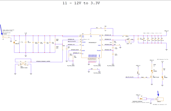
See below picture from my schematic.
When I connect 3.3V to J4 on my board, and nothing is connected to Vin via J3, I measure 3.3V on Vin pins of the MPQ8634B.
Q1: Does it allow to place 3.3V on SW pin (SW pin via L2 ) without supply Vin?
Q2: Where does the 3.3V on Vin come from if I do not connect power supply to J3 ? Is it from internal connection between SW pin to Vin pins inside the MPQ8634B?
Thanks,
Avi.
Hello Avi,
To answer your questions:
- An inductor will behave as a short in DC. Although it is possible to apply 3.3V at the SW node via L2 I would not recommend as it is outside the operating parameters of the part and could damage internal circuitry.
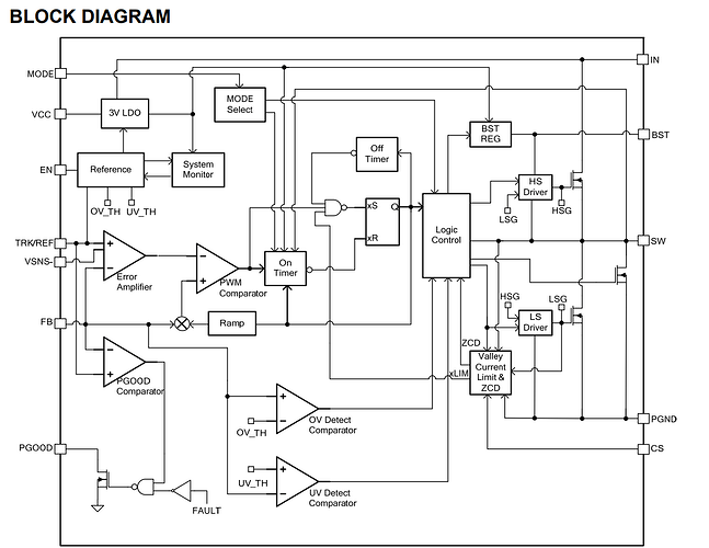
- If the High Side Gate is turned on, the power flow will enter the SW pin and be connected to the IN pin. See block diagram below.
Thanks for the answer.
Please close the case.
Hi Stephen,
- in my design I just need to remove L2 in case I supply 3.3v from J4 ? Do I need to remove also R259 and C209 ?
- I want to try fix this in redesign. Any idea how I can do it without the need of removing components ?
Thanks,
Avi.
Hello,
No you do not have to remove the feedback network from your design. The reason MPS would not recommend applying an external 3.3V is primarily due to the uncertainty of how the internals will behave. An unwanted protection may be triggered and can result in unexpected behavior.
As a solution for your redesign, simply adding a diode or FET in series with the output lines (most likely after C8) will allow for power to flow out of the converter only and protect the IC from seeing an external voltage at the input.
Got it, Thanks for the solution !

