Hi,
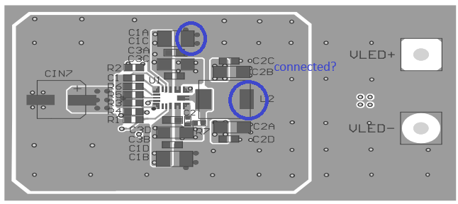
I want to implement MPQ7231 LED driver reference design and noticed something i cant explain: In both the schematic (Figure 11) and PCB layout, the LED+ output (L2 output) appears to be connected to GND.
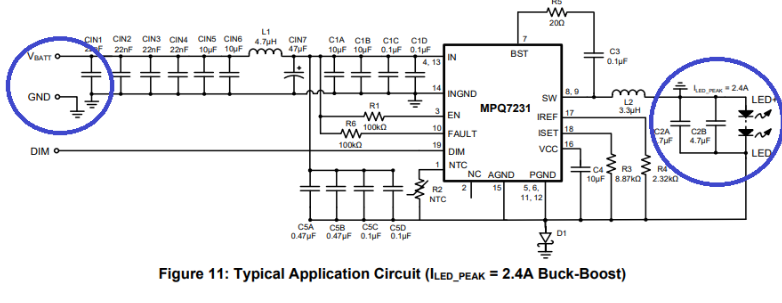
Could you please explain how the buck-boost topology achieves proper LED driving with this configuration? Specifically, I’m interested in understanding:
- How the current regulation works when LED+ is at GND potential
- If LED- operates at a negative potential relative to GND
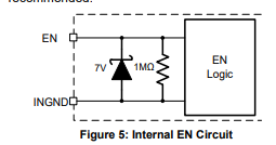
Other question regarding EN Pin Voltage:
The datasheet specifies EN pin maximum voltage as 5.5V, however, the typical application shows EN connected with a resistor to VIN with Abs. max of 50V. The internal zener diode is specified to regulate at 7V. This seems to create a window where the EN pin could be damaged.
How is the EN pin protected in applications where VIN > 5.5V?
Thank you for your clarification.
Best regards,
Timo