We are currently performing CISPR25 Class 5 conducted emission testing on our DUT and observed some emission concerns that we would like your guidance.
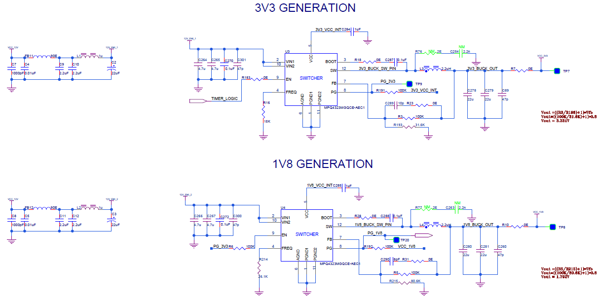
The DUT uses MPQ4323MGQCE-AEC1-Z buck converters for 3.3 V and 1.8 V generation. The overall power architecture is based on MPS buck converters and LDOs.
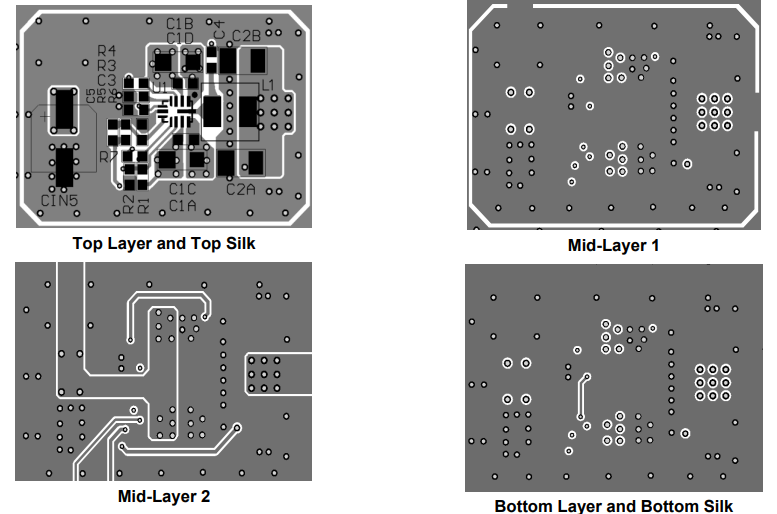
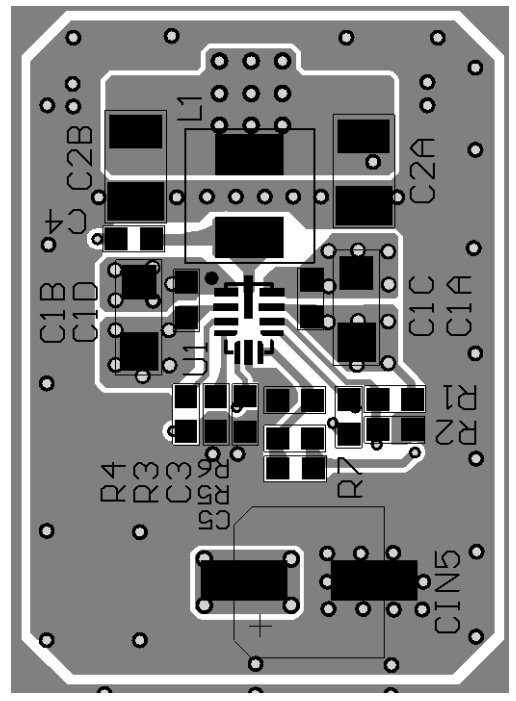
Attaching the buck converter schematics for reference.
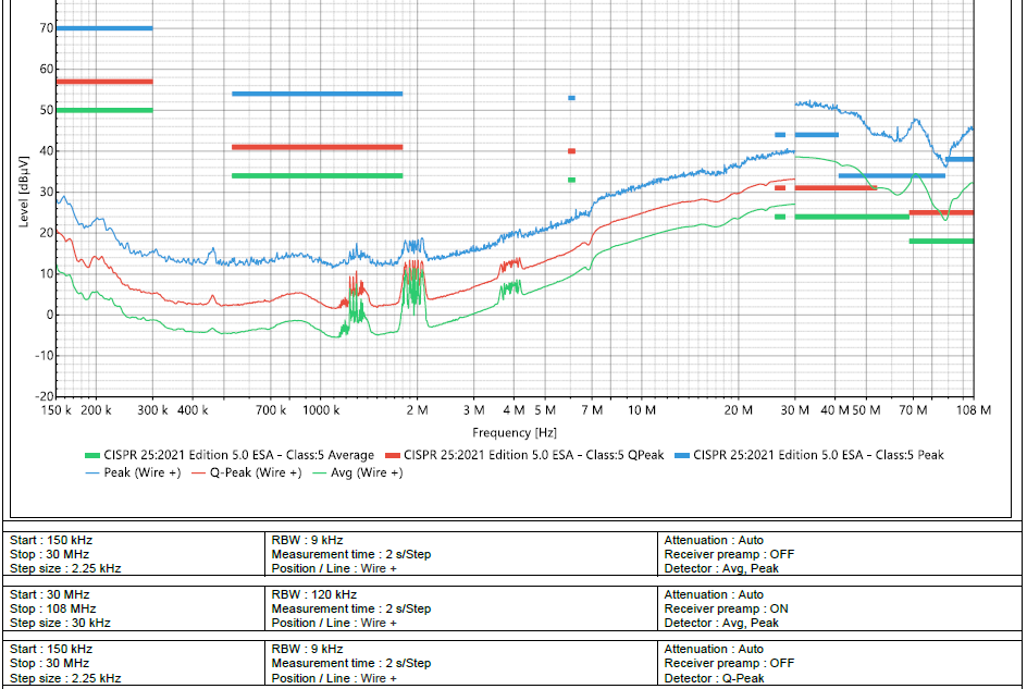
CE Test observations:
Failing peaks observed in the low-frequency band, suspected to be related to the switching regulator fundamental and harmonics. (test results attached).
I feel that it would be more helpful to provide ways in improving your EMI performance if we perhaps took a look at images of your layout with these ICs. Hoping to hear back soon.
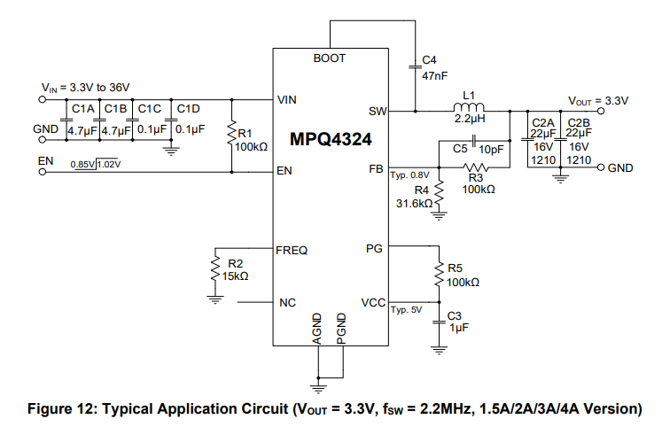
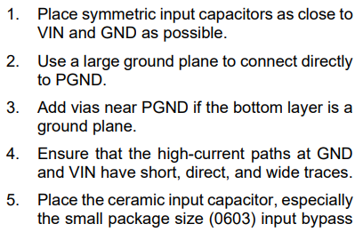
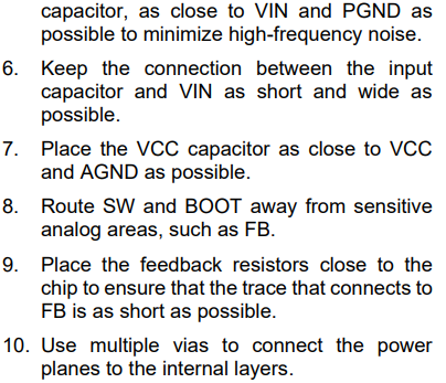
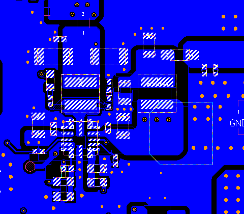
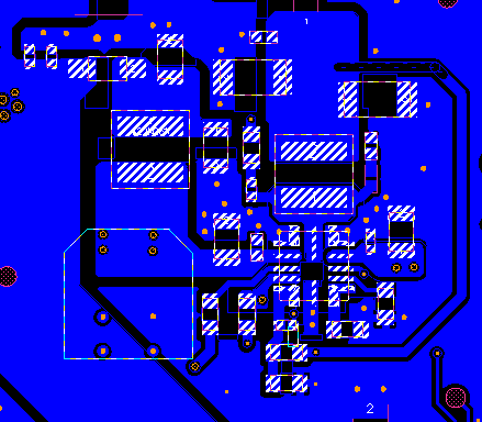
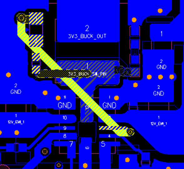
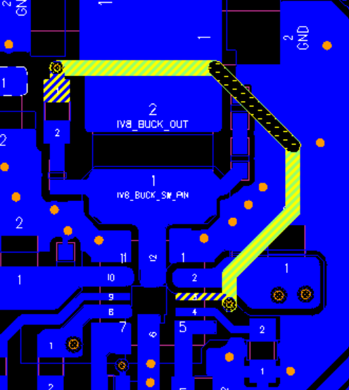
For both layouts, I will make my comments with respect to the top power plane as shown in the PCB Layout Guidelines. Here is a zoomed in image of this:
Your layout could be more symmetrical here. I can see that you did this with Cin on both sides for the 1.8V and 3.3V layouts. However, trace widths could be further minimized here. Also are the SW and BOOT routed away enough from sensitive analog areas?