Dear MPS Technical Support,
We are currently using the MPQ2484UGF-AEC1-P for an LED lighting application in PWM dimming mode. Our operating conditions are as follows:
-
PWM Frequency: 40 Hz
-
ON Time: 1 ms
-
Input Voltage: 12 V
-
Load: 10 LEDs in series
-
Output Voltage: ~60 V
-
Output Current: 600 mA
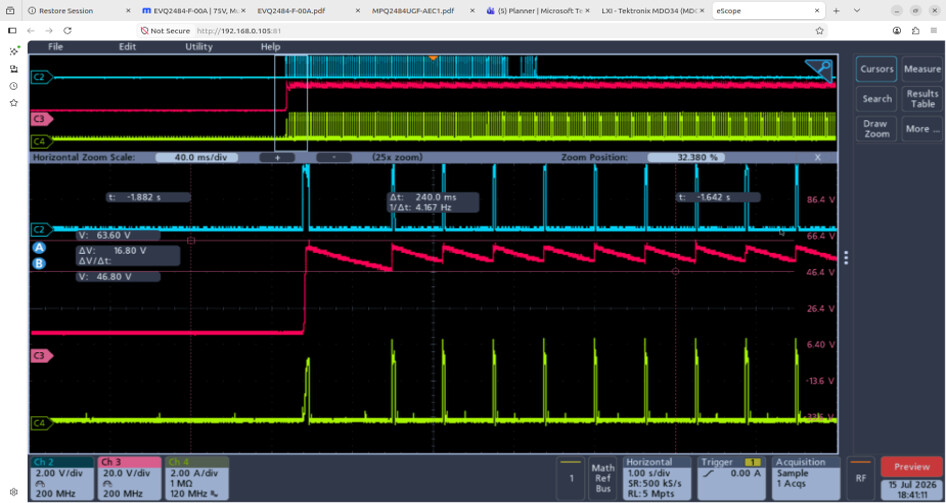
During the first PWM pulse, we observe a peak input current of approximately 9 A, which causes the driver to enter fault mode. During subsequent PWM pulses, the input current settles to approximately 4 A.
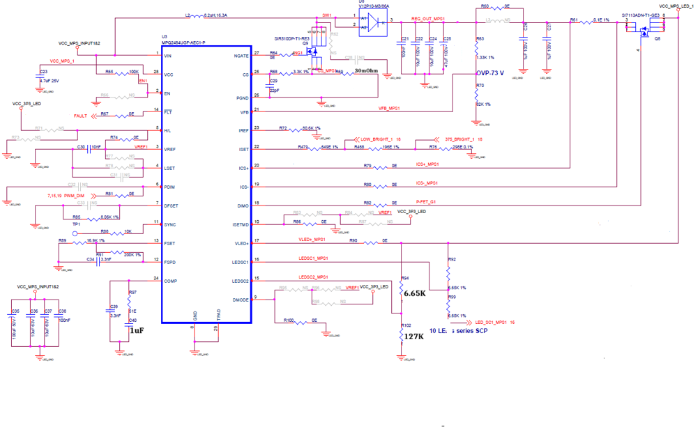
Schematics:
Input Current:
To reduce this transient current, we performed several trial-and-error modifications by reducing the output capacitance and increasing the compensation capacitor. Our observations are summarized below.
Trial 1
Design Changes:
-
Unmounted C25 (47 µF), resulting in a total output capacitance of 22 µF.
-
Increased the compensation capacitor C40 to 2 µF.
Observations:
-
Initial pulse input current reduced from 9 A to 4.5 A.
-
A delay 50uS observed to settle the output current to 600mA
-
The steady-state input current increased to approximately 4.7 A.
-
Blue - PWM RED- Output Capacitor Voltage Green- Input Current
-
To mitigate Observations 2 and 3 from Trial 1, we performed another set of modifications as described below.
Trial 2
Design Changes:
-
Unmounted C21, C22, and C24, resulting in a total output capacitance of 49 µF.
-
Increased the compensation capacitor C40 to 6 µF.
Observations:
Initial pulse input current reduced from 9 A to 5.2 A.
-
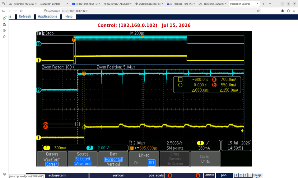
The delay between the PWM signal going HIGH and the output current reaching 600 mA reduced significantly to approximately 680 ns.
-
The steady-state input current decreased to approximately 4 A.
-
However, the output current ripple increased compared to Trial 1.
-
BLUE- PWM; YELLOW- OUTPUT CURRENT
We would appreciate your guidance on the following:
-
Based on the above results, which of the two compensation approaches is likely to provide better loop stability?
-
Could you please explain the recommended method for selecting the RC compensation network (COMP pin components) for the MPQ2484UGF-AEC1-P? We could not find any design guidelines or compensation calculation method in the datasheet.
We look forward to your recommendations.
Attached Waveforms and Schematic for your understanding
Thank you for your support.
Best regards,
Hello,
I’d firstly like to say that this is an excellent test flow, thanks for providing the schematic, waveforms, and easy to follow steps per test trial iteration.
Generally, if you want to minimize the output current ripple, you should perhaps stick with your initial 69µF output capacitance.
There are no exact formulas for the COMP components since this heavily relies on initial conditions, which can vary for a multi-topology part like this. You will have to tune this with the same process flow you are performing now. It all has to do with balancing the poles and zeroes to stabilize the control system, and you have already taken the right steps.
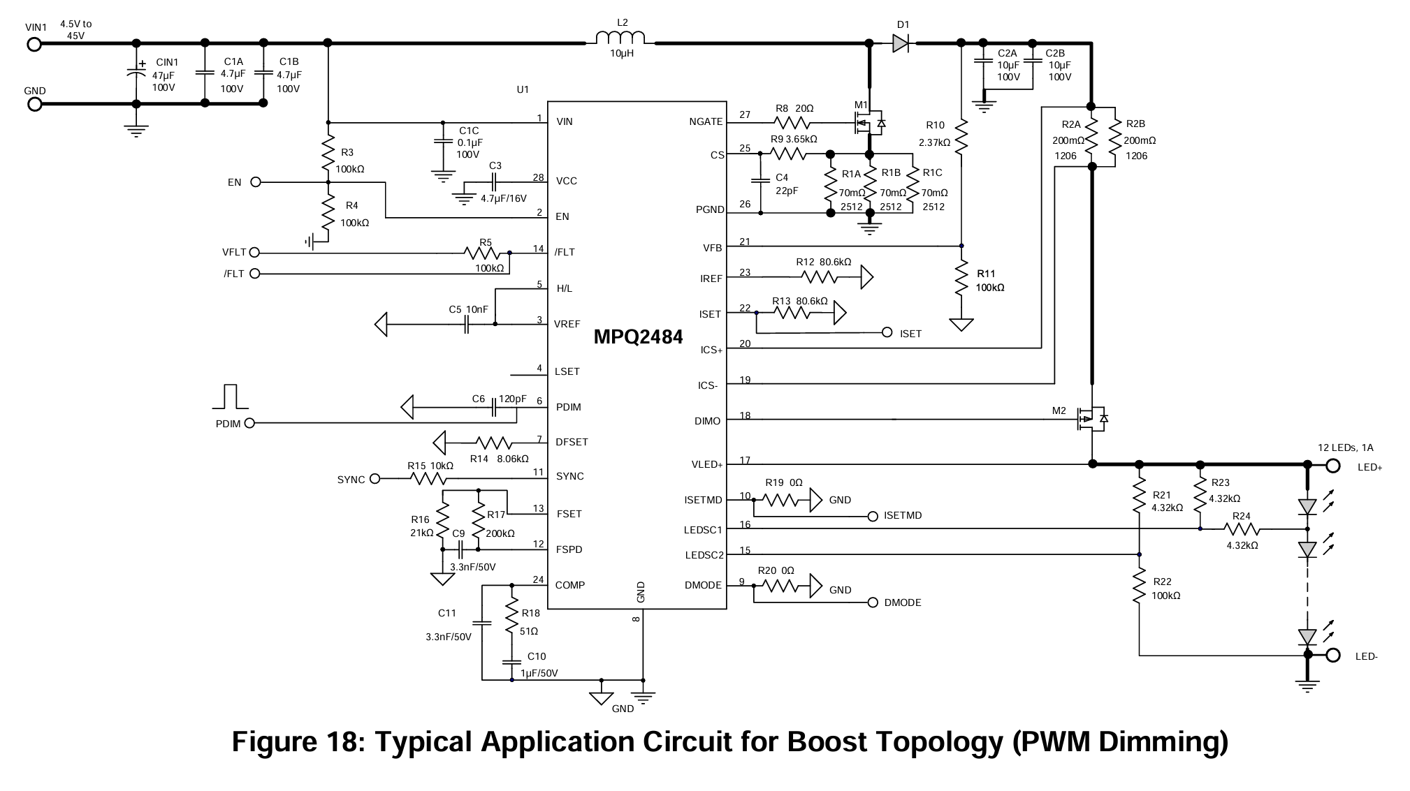
Here is the reference schematic that I will be comparing your schematic against:
I will review these schematics soon. In the meantime, any updates on tuning?
Hi @@Krishan.FAE ,
Is there any excel design calculations for this IC
Hello,
There are no excel design sheets for the MPQ2484. However, we do have an MPSmart model on the MPQ2484 posting on the MPS Website on the Design Resources tab.
You can also download MPSmart v9 for free.
Best,
Krishan
Hi @Krishan.FAE ,
Thanks for your valuable reply.
I would also like to discuss one observation with your design team. After removing C25 (47 µF) and fine-tuning the compensation network by changing C40 to 1 µF, we no longer observe the inrush current issue with the following operating conditions:
Since the inrush current issue has been resolved by removing C25 (47 µF) and adjusting the compensation capacitor C40 (1 µF), we would appreciate it if the MPS design team could review this compensation change.
Specifically, could you please help verify:
- Whether the control loop remains stable across the specified input voltage range and operating conditions.
- Whether this compensation adjustment introduces any concerns related to stability, transient response, or reliability.
- Whether this solution is considered acceptable for production, or if you would recommend any additional modifications or validation.
To properly evaluate the stability of the control loop, you would need to run a transient response at the worst-case loading conditions. Minimizing the overshoot, undershoot, and any oscillations to settle the output voltage here would be a good metric of a stable control loop.
If the overshoot, undershoot, and settling time are to your spec, this would be a valid design that would be acceptable for production.