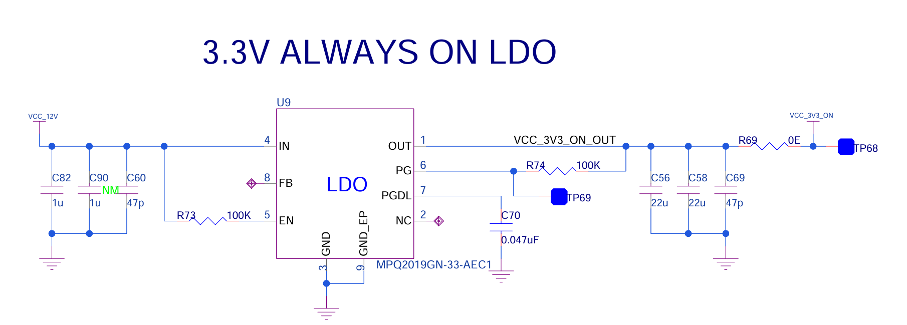
Hi Team, I would like to use the MPQ2019GN-33-AEC1-Z in our design. Our Vin(max)= 18V, Vin(min)=10.5, Vin(nom)=13.8, Vout=3.3V, Load current is 20mA. Kindly review it and let us know any feedback on the same.
Hello again Abdul,
This schematic coincides with typical application, no apparent issues that are seen on this schematic since this is the fixed 3.3V version with internal resistors. Please keep the following layout guidelines in mind:
-
Place input and output bypass ceramic capacitors close to IN and OUT, respectively.
-
Ensure all feedback connections are short and direct. Place the feedback resistors and compensation components as close to the chip as possible.
-
Connect IN, OUT, and especially, GND, respectively, to a large copper area to cool
the chip. This improves thermal performance and long-term reliability.
Hopefully this helps and provides insight.
Best,
Krishan