Hello Support Team
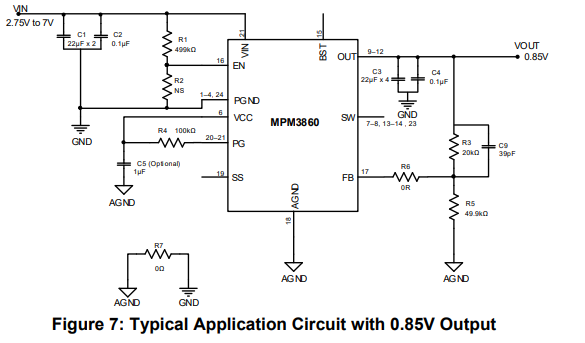
I’m confused a bit about typical application circuit (see fig above):
- Why R1 is used? Is it an external UVLO set point (with integrated 3.3M pull-down)? In the DS I can see that UVLO is already built-in in the device. Can I just tie the EN pin to VIN?
- What is the purpose of 0Ohm R6?
- What is the case to use C5?
- C9 is used to increase regulator phase margin?
- Should I connect some snubber circuit to the SW output to decrease the noise?
- Is this an issue to form a voltage divider with R1 = 10k, R2 = 24k?
Thank you in advance
Hello Ivan. See answers below:
-
 ; you can tie EN directly to VIN and support up to a 7V input voltage
- R6 is used to fine-tune noise immunity of signal going to the FB pin; set as 0 Ohm for now but depends on layout of board if it may need to be stuffed
- Even w/ an internal 1uF for VCC, if additional decoupling is needed, C5 is recommended
- C9 used as a feedforward capacitor to help w/ transient response
- Typically not recommended but can leave snubber footprint if SW node causes any noise/ringing issues
- Shouldn’t be an issue; if design requires to disable device when a certain VIN is needed, can size R2 such that a voltage divider will cause voltage seen at EN pin to be below threshold required to enable device
Hi Christian!
It’s clear, thanks!
Hi @christian.cross,
Can i use a EVM3650-QW-00A layout as a reference for MPM3860?
Hi ivan.mazur,
The MPM3650 and the MPM3860 are different parts. Please follow the PCB guidelines on pg 17 of the MPM3860 datasheet for help.
Thank you,
Vinh Tran
Field Applications Engineer
Hi Vinh,
Thank you! I will follow the MPM3860 DS. Please note that the recommended PCB layout (figure 6) in the MPM3860 DS has several inaccuracies:
-
BST pin on the reference schematic leaved floating, but on the layout example its connected to somewhere thru the via
-
VIN/VOUT PGND on the top layer are not separated as mentioned in Guideline #8
Best Regards,
Ivan