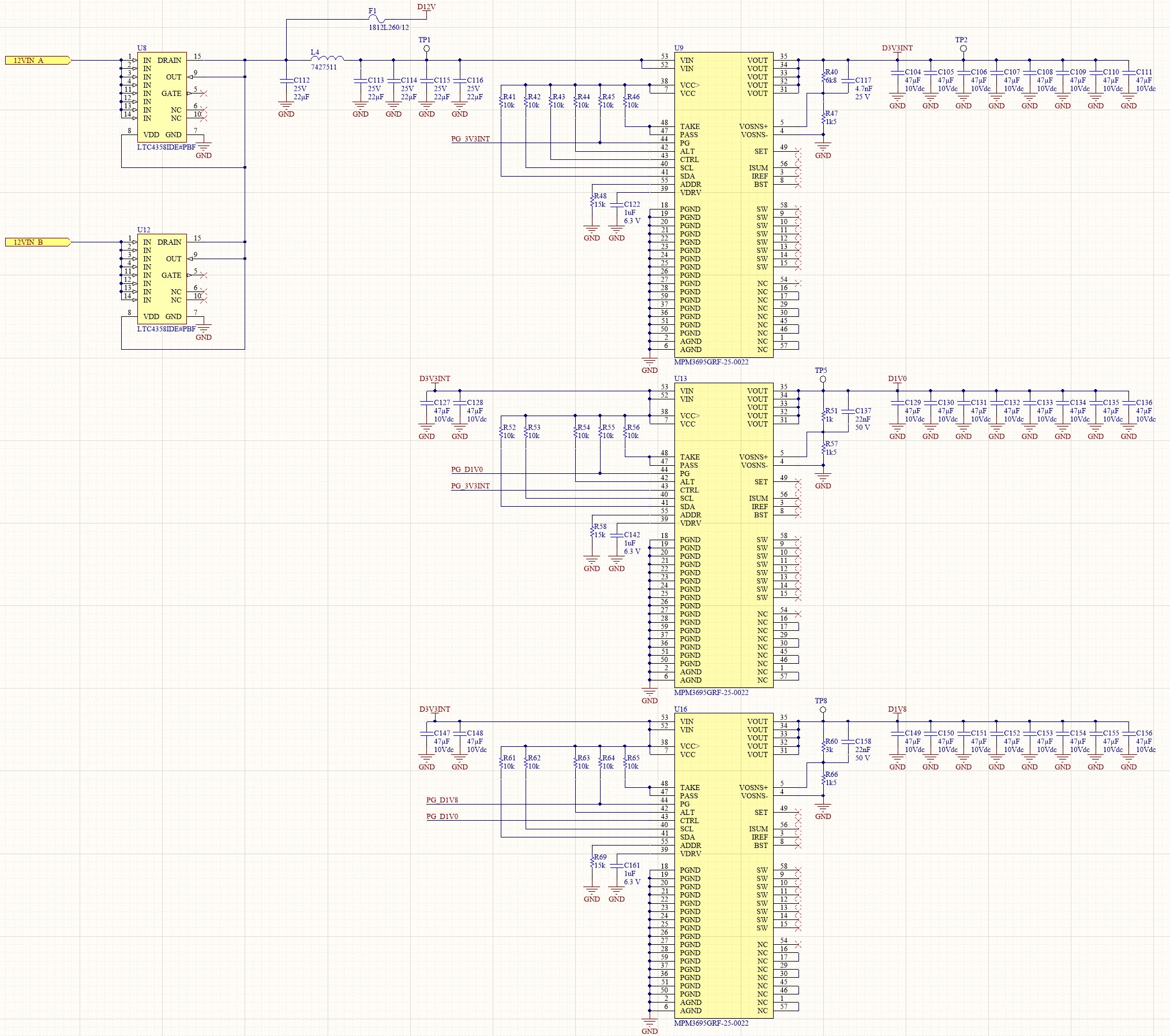
Hi, I have a design based on Fig 6 in the MPM3695-25 datasheet where the device is powered by a single 3.3V input. The only difference is the values and numbers of input and output capacitors used, but they amount to more or equal the capacitance shown in the figure.
The device does not turn on! Has anyone had similar issues and resolved them?
I got it to work! It seems like the externally powered vcc mode does not work unless the input voltage is >= 4V. Then fig 6 of the data sheet is wrong. Also the text describing input voltage range from 3V is wrong or compleytely untested. Maybe an applications engineer could shed some light on this?
Hello Jens,
Thank you for bringing our attention to this. I will let our internal team be aware of this and update the datasheet accordingly. Please let us know if you have any more questions!
It would be really nice that you instead of changing the datasheet, provided a solution for it to work from 3.3V as I would have to redesign my board to match the 4V limitation.
Hi Jens,
May I ask what the specs are for your input capacitors? This figure should be actually correct since the Vcc is pulled up with the external supply.
I am attaching the design. The D1V0 rail and the D1V8 rail do not start. It works if I trim the D3V3INT to about 3.92V
Hi Jens,
Thank you! You may also send this schematic and layout files to mpsnow@monolithicpower.com for further assistance. From what I see initially, the feedforward capacitor for the D1V0 and the D1V8 can be changed to the recommended value of 33nF. Are you using I2C communication with each of these devices? If so, the addresses should also be different (different ADDR resistor values).
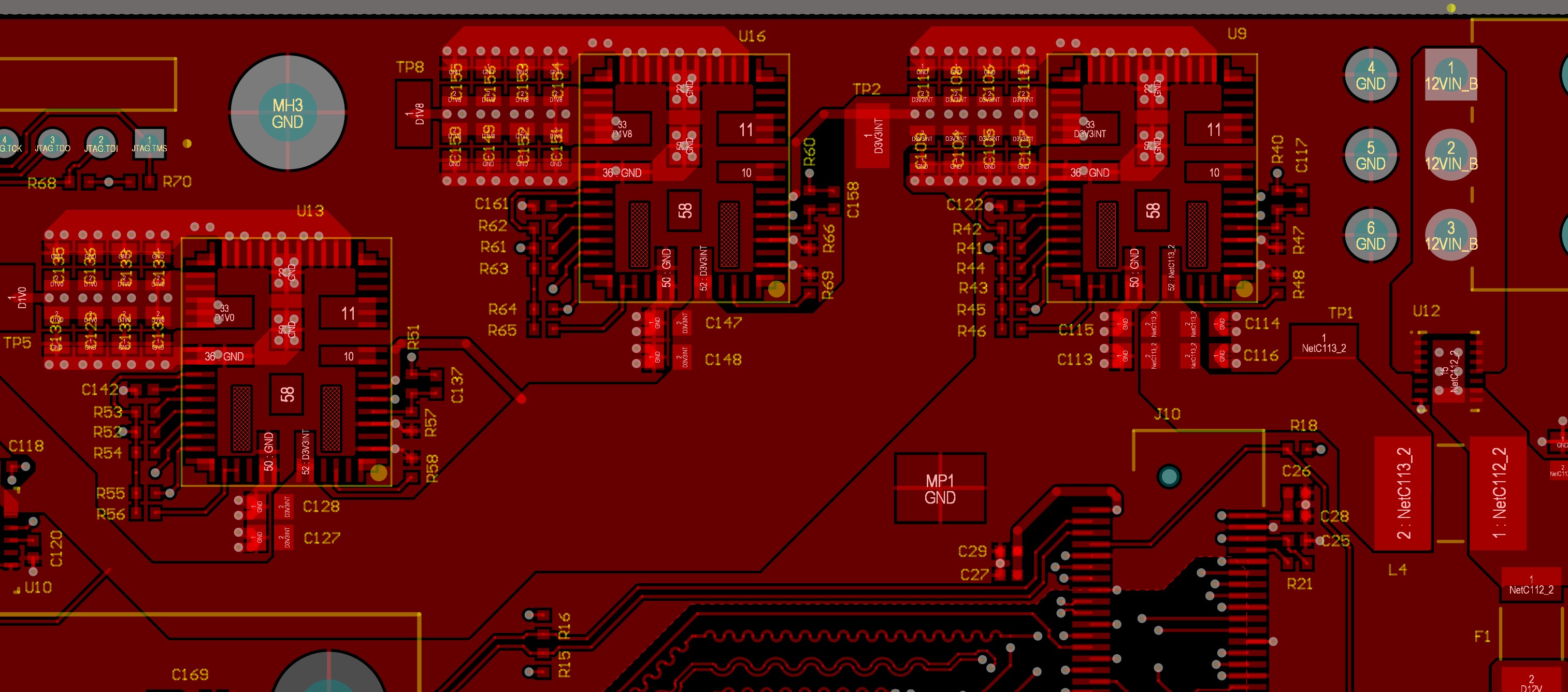
Can you also send layout files for our team to help check? We prefer Altium, any cad, or .brd files but we can also work through gerbers too.
I am attaching the top layer of the design since all of the power traces are routed on the top layer. All grounds are conneced directly through vias to at least 2 ground planes (it is an 8-layer board)
Thank you Jens. What currents are you running these devices at?
Let me take a look and give you any comments if I have any.
Are you also getting any voltage reading on the Vin of the D1V0 or the D1V8?
The current delivered by the D1V0 is about 3A average but could be higher depending on the code running on the FPGA it powers but not more than 5A. D1V8 is 2A and since the D3V3INT is powering both the D1V0 and D1V8 converters the current would be ~2A for the D3V3INT. Well below the limits of either converter.
As I stated before, the D3V3INT rail works perfectly at the nominal 3.3V. This rail powers the 1V and 1.8V converters configured for external VCC as in fig 6 of the datasheet.
The issue is that I have to trim the 3.3V to 3.92V to get the 1V and 1.8V converters to start. Luckily I do not have any devices apart from a DDR3 sodimm that uses the 3.3V rail. The sodimm is currently not installed so I can get away with 3.92V on the 3.3V rail. However I would like to know what is wrong, my design or the datasheet.
Hi Jens,
I am not finding any issues on your schematic nor the layout. Could there be any current dips or transients that would make the 3.3V dip below 3.12V (this is the external Vcc’s lower limit)? Are you able to send scope captures of the input, output, and SW for us to help diagnose?
Also, I am curious as to why you chose a high current device such as MPM3695-25 for rails that run under 5A. Are there situations where you expect high transients and were accounting for that or they are used to power other rails downstream from the 1V and 1.8V?
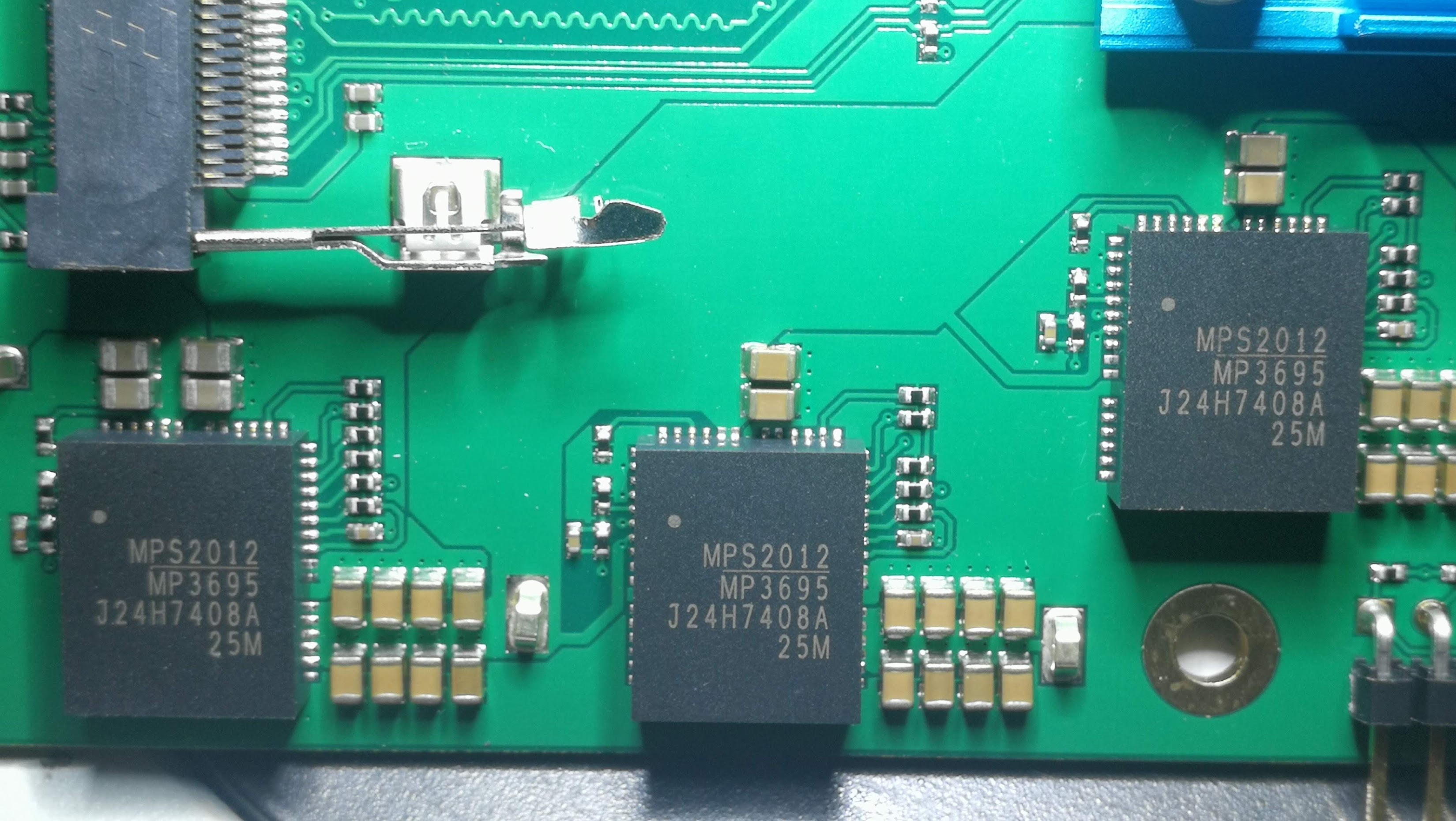
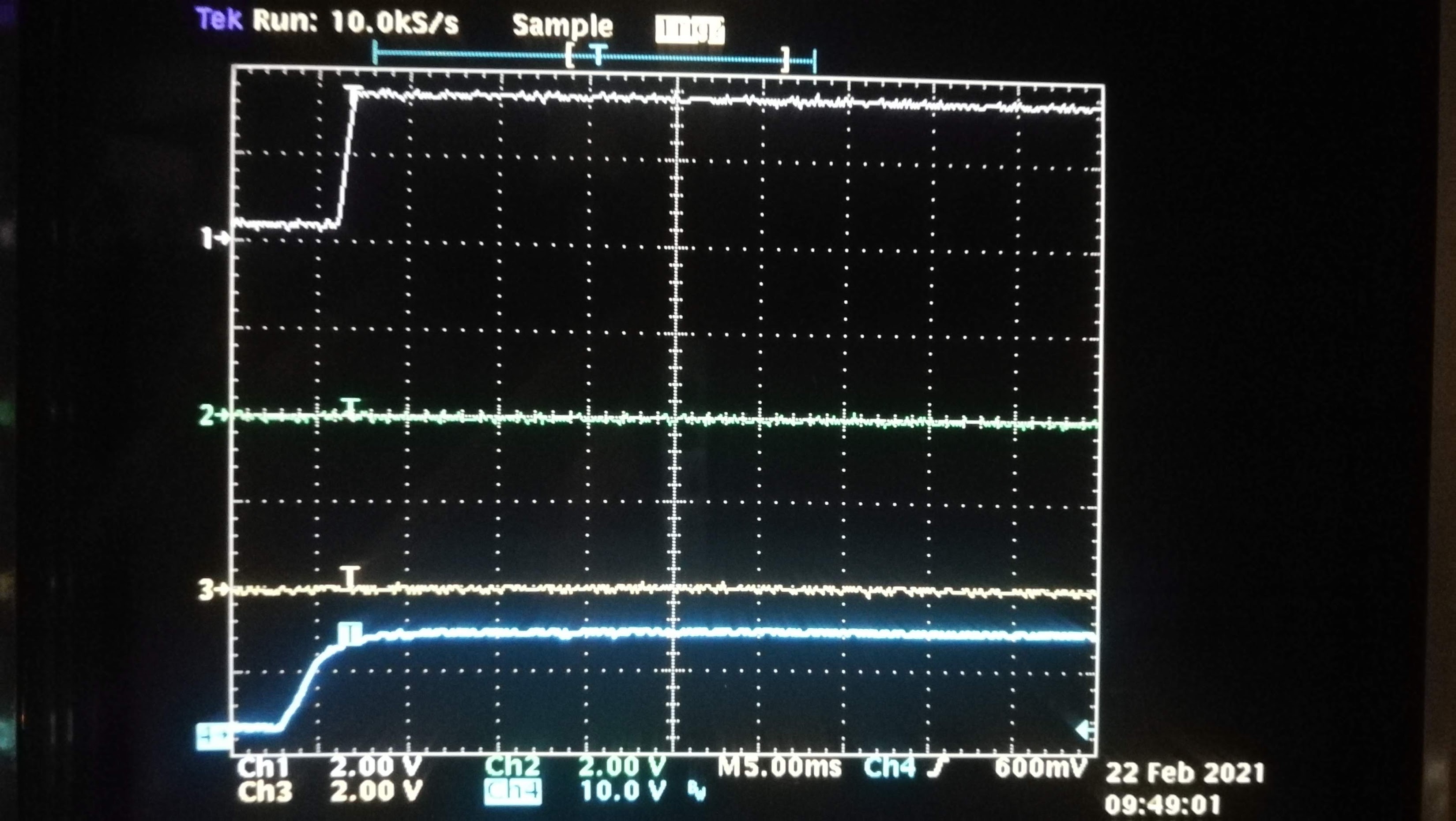
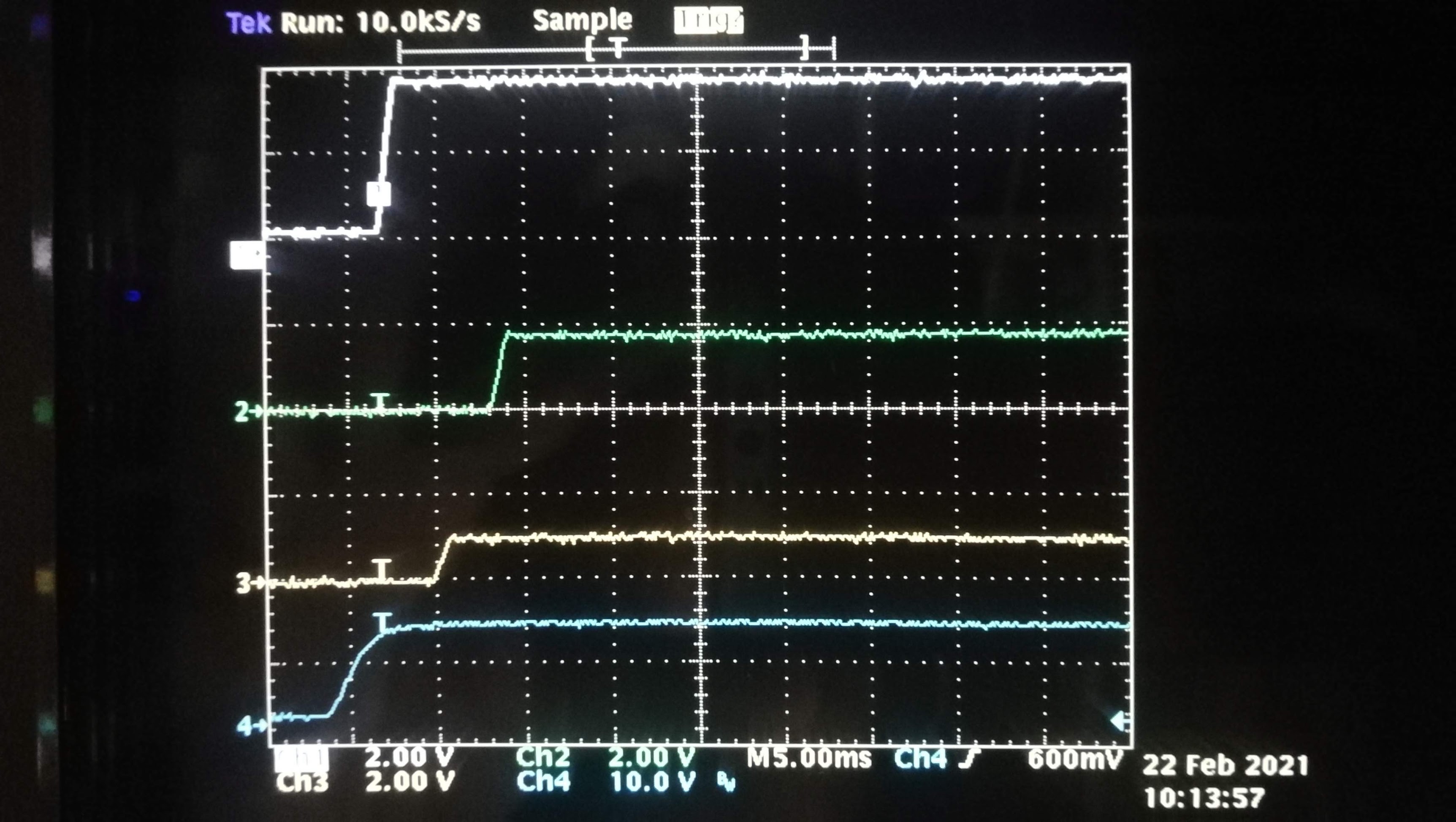
The reason for choosing the MPM3695-25 was I needed a design that will be able to handle future needs. Since there probably will be processing capability upgrades to the FPGA and other parts of the design. I am attaching a picture of one of the boards so you can read the serial numbers and also oscilloscope startup pictures. Trace 1-4 are 1: D3V3INT, 2: D1V8, 3: D1V0, 4: 12VIN at U9. The first picture is without the 3.92V fix and the second is where all rail starts after the fix.
Hi Jens,
Thank you for sending those. I went back into the datasheet and found that since you are using -0022 part number, the default for VIN_ON is 4V. That means you will have to get into that register (35h) and change that lower than 3.3V. You will need to change your address resistors on each of the 3 MPM3695-25 to be different to communicate to adjust this register. You can then save this through MTP so that upon each power cycle, it will have this register value saved.
Ok, thank you for clarifying. In my humble opinion fig 6 should really mention this is not standard operation. Are you planning on releasing a version wich has 3V as a standard setting, and if not how many would I need to buy to get the 3V limit set from factory?
Hi Jens,
We have other -#### parts that should have the 3V setting. Can you please send an email to mpsnow@monolithicpower.com about this part? We will get in contact with our factory to find the exact part number to send you and also get a sales person to be in touch with you. Thanks!
Hi Cecilia,
This is a new board for a product we plan to release in a year so there is no immidiate need for a large number of devices. I will have time to adjust the design to match the defaults in the -0022 device. Also since it works by simply raising the 3.3V it suffices for now. Thank you for all your help!
Best regards
Jens
Hi Jens,
No problem! If you are ever in need of samples or technical assistance, please feel free to reach out to us and we are happy to help out!