We are designing a 6-layer PCB.
We plan to use the MPM3620A component and have a question regarding the PCB pattern.
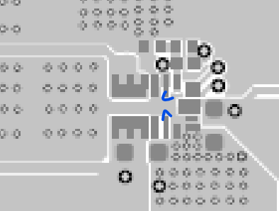
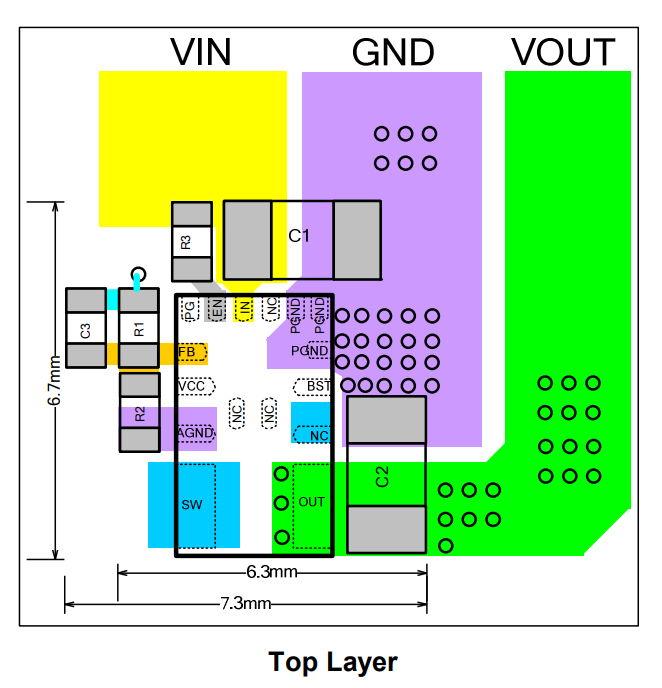
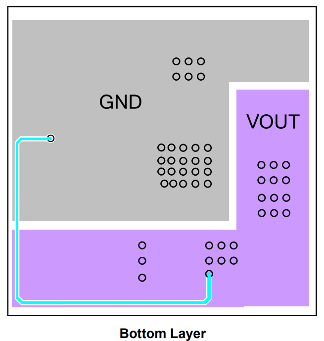
Regarding the keep-out zone for pins 19 and 20, is it sufficient to simply leave that area clear of pin pads, metal traces, and via holes, like not a contact pad and then fill it with GND copper?
Or do we need to create a GND cutout in that area on the component mounting layer?
Alternatively, should we cut out that area on all layers?
We observed that the EVM3620A fills that area with GND copper.
I would say it would be best to fill the area with GND copper for pins 19 and 20. If the EVB has corroborated this as well, then feel free to continue to use this as a reference.
Given that the datasheet also contains a phrase like: ‘SHADED AREA IS THE KEEP-OUT ZONE. ANY PCB METAL TRACE AND VIA ARE NOT ALLOWED TO CONNECT TO THIS AREA ELECTRICALLY OR MECHANICALLY.’, I will proceed by filling the surrounding area with GND Copper, ensuring no electrical or mechanical contact to the keep-out zone.
Please note, I haven’t physically checked the EVB (Evaluation Board) yet; I only saw the attached layout in the EVB datasheet."
The reference you provided seems to suggest that the Copper on the Top Layer around the ‘NC’ (No Connect) pins is left void/cleared.