Hi, I have a problem with MPM3612 layout and I don’t know how fix it. I have 7,4V to 9V for input and I want 5V to output. I use R1=1613k and R2=220k to configure output and use a 22pF capacitor to stable Vf as schematic examples. But nothing works. To discard soldering and footprint issues, I test it with version MPM3612-33 that has same footprint and without divisor resistors and it works perfectly. Vout has 3,3V as MPM3612-33 says in datasheet.
I found in datasheet that if some issues happends, device will responds with 0,6V on Vout.
I will share you some images with layout and schematics.
Best regards and thanks in advance,
David
Hi David,
Welcome to MPS technical forums, sorry to hear that your facing issues with MPM3612.
MPM3612 has two versions, ‘-33’ is a dedicated fixed 3.3V output voltage version, whereas the one used in your design is an adjustable one.
Looking at the schematic it looks OK overall, what is the Vout you are observing and what load current?
Can you share some waveforms such as Vin & Vout?
Regards,
Adhish
Hi, thanks for your response,
My load current is only 40mA to supply two ADCs (ADS1158IRTCR)
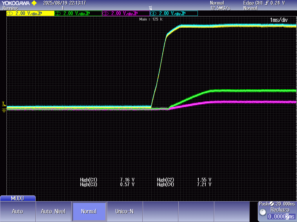
And this is the response viewed on own oscilloscope:
Where Blue is
Ven pin(1), Yellow is
Vin pin(2), Green is
Vout pins(4-5) and Violet is
Vfb pin(6)
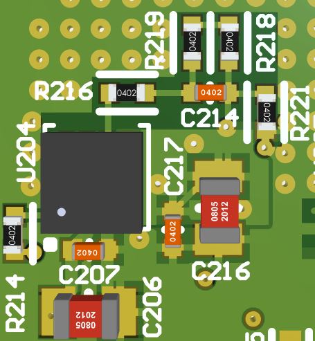
Also I include the distribution of components on PCB board:
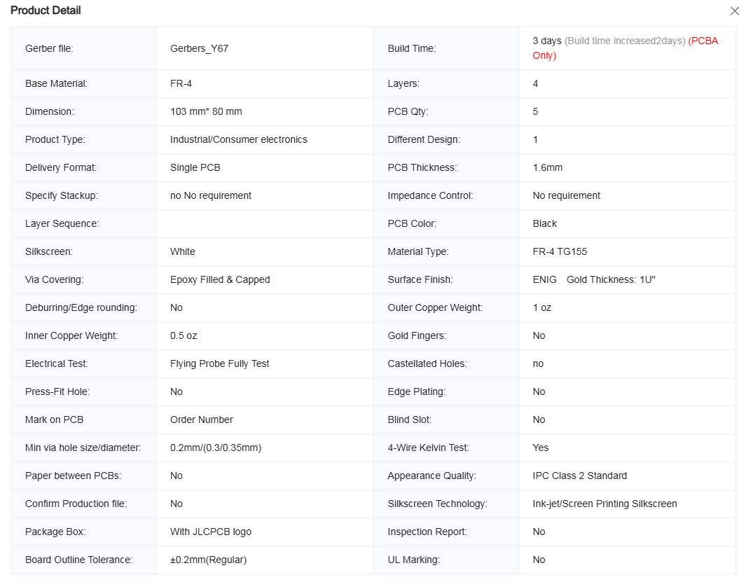
At the end, I want to include fabrication information about weight of layers, FR4 type and number of layers in case it helps too:
Best Regads and thanks in advance,
David.
Hi David,
Apologies for the delay in getting back to you.
- Looking at your schematic, it looks like there is a missing decoupling capacitor for Vcc pin.
- Secondly, the 0 ohm resistor must be connected to the junction of the two feedback resistors, currently in your design it is connected to Vout rail. Kindly correct this as shown in our EVB datasheet for this part. I missed this before.
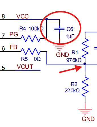
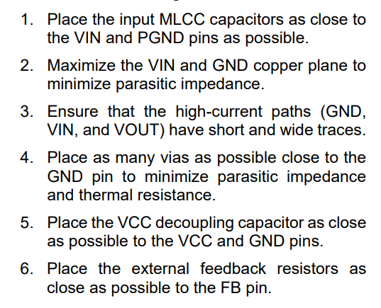
After looking at the layout, your feedback resistors are not close to the IC pin due to every component placed in the top player, which is not as per recommended in our datasheet.
Kindly follow the layout guidelines as mentioned in our datasheet and EVB.
Regards,
Adhish
Hi David,
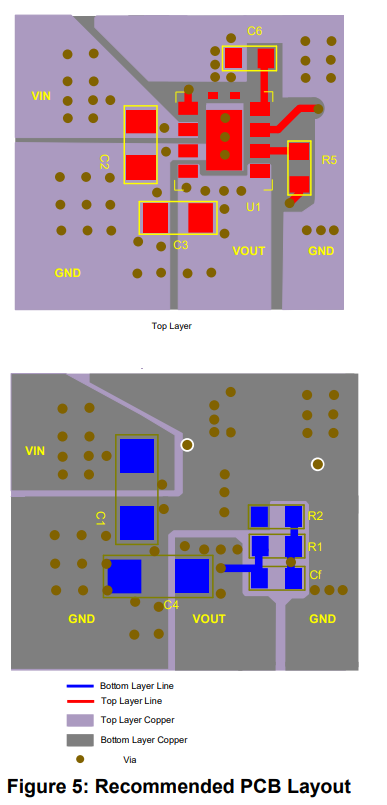
I am attaching our EVB PCB layout here as well for reference that you can take a look at. Its a 2 layer board.
Regards,
Adhish
Hi,
Thanks for your response,I managed to solve it, in the end it was what you said, I put the 220k resistor between the FB pin and the GND because my design did not have a voltage divider and therefore the output delivered an erroneous Vout.
David.
1 Like