Hi,
We are using MP9928 for our application as current source. I am unable to get frequency at Freq pin. And ho to calculate inductor value.
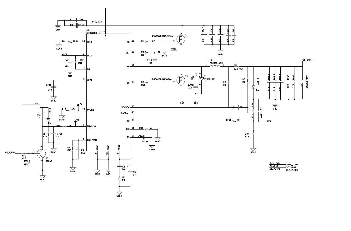
Application is Input 12V, output 1.5V@10A. Freq selected 200KHz 100K resistor connected at pin no 10. Inductor used is 4.7uH. Problem is that 10A current is not reached max is 9.5A and it is not in CC mode means output voltage drops to 0.6V when 10A is flowing through load.
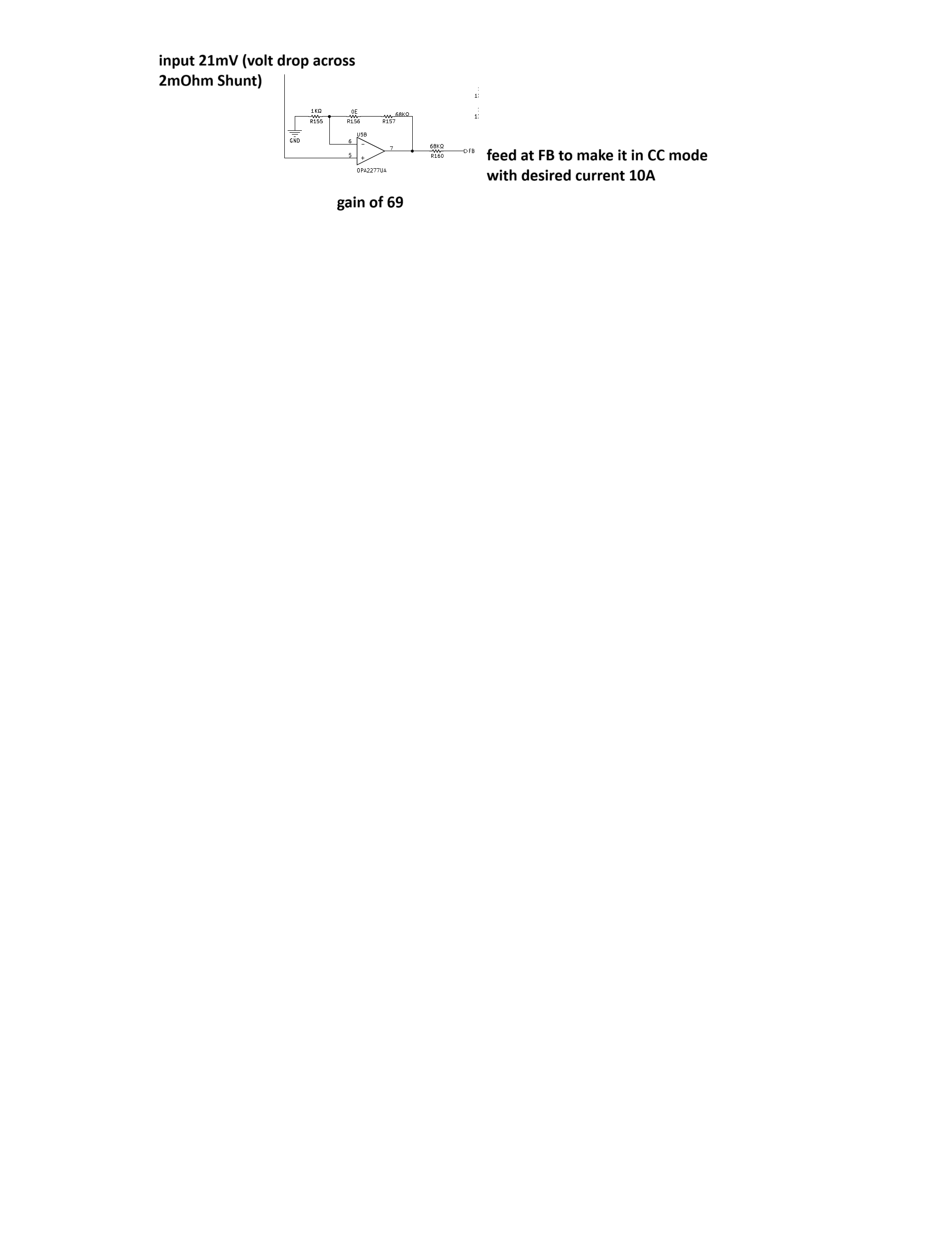
For Feedback voltage and current, for volt feedback diode is used and for current feedback OPAMP is used (drop across shunt feed to FB pin). The same design works well in other reference model.
Hi @MOHAN,
Thank you for posting to the MPS Technical Forum! I have a few questions about your application:
What frequency are you seeing instead of 200kHz?
How did you calculate your COMP pin values and feedback pin resistors?
Are you doing these tests on your own PCB or with an MPS evaluation board?
Thank you,
Isabella
Hi,
I have 1 working reference unit in that this circuit is used.
- Reference design
a) Frequency in reference unit is 200KHz
b) inductor value is 6.8uH.
c) Output volt is set to 1.5V,
d) Current is 10.2A.
Where as in my PCB
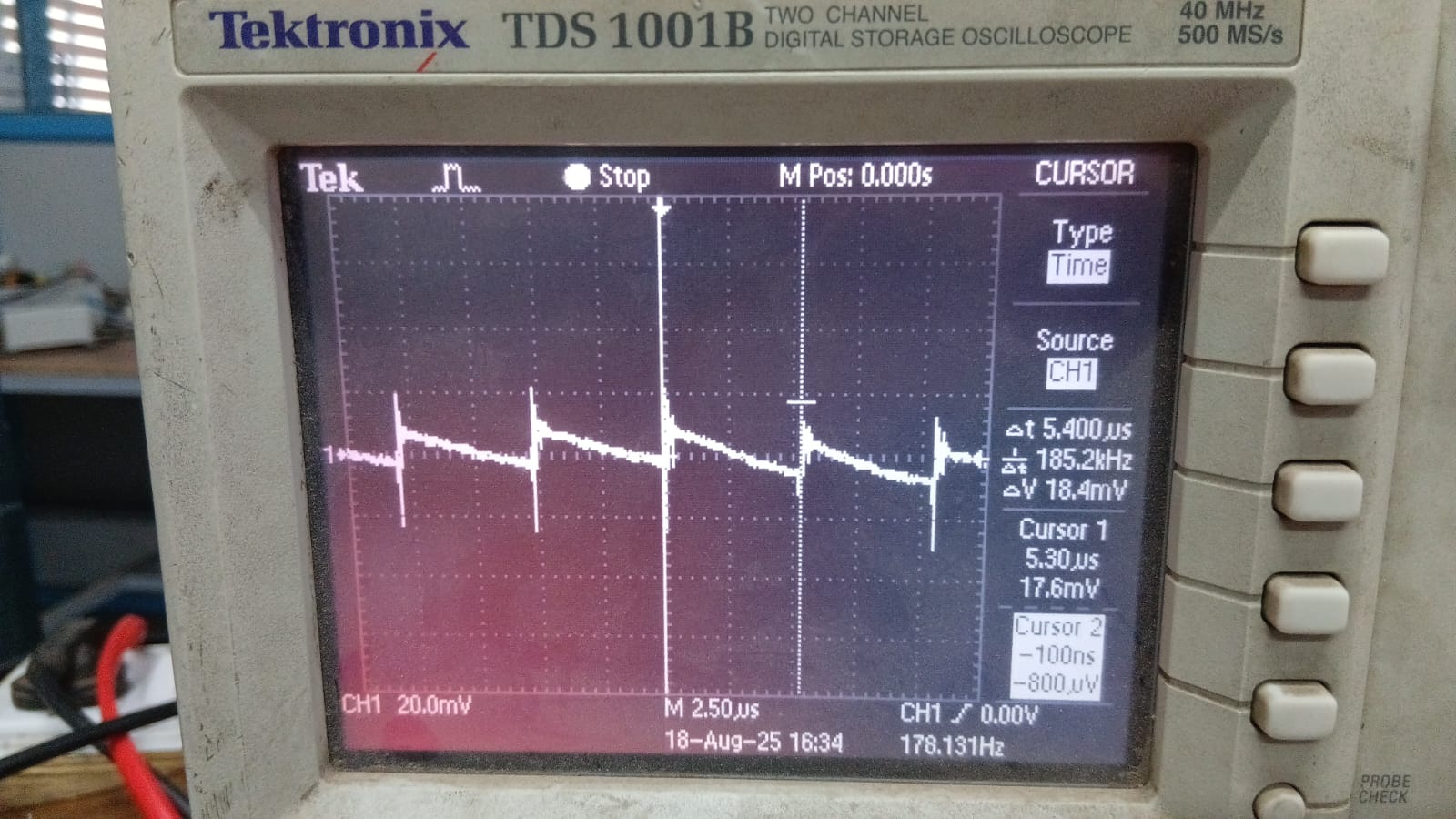
a) Frequency is straight DC Line, amplitude 200mV
b) Inductor 6.0uH.
c) Output is 1.5V dc.
d) Max Current is 9.5A only.
e) COMP pin values and feedback pin resistors is same as reference unit.
PFA reference design frequency waveform.
How to design COMP components
Just to clarify, do you have one physical reference design unit that is able to output your desired current of 10.2A, but you aren’t able to replicate it with your own PCB? Is the schematic from your first post the same for both your reference unit and your PCBs?
One additional question, if you’re not seeing a frequency on the FREQ pin of your design, are you seeing the 200kHz frequency on your SW pin at all? Thank you.
Hi,
Yes schematic is same for physical reference design and our own PCB.
- PFA see the current feedback at FB.
- Freq at SW pin
PFA without load condition and with load condition
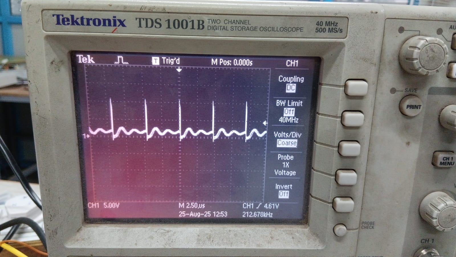
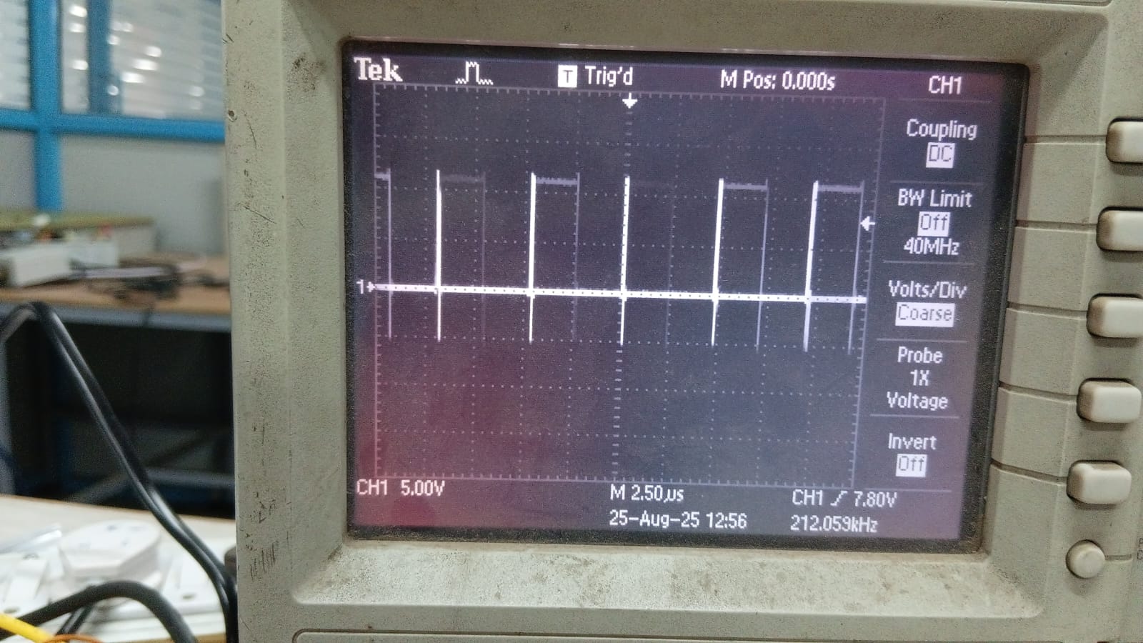
While in physical reference design unit at load condition waveform is clear and in our own PCB there are some hidden line/noise.
Hi Isabella,
Is it possible to share your mail ID? I will send the complete schematic, layout, and working details.
Regards,
Mohan
This topic was automatically closed 90 days after the last reply. New replies are no longer allowed.