Hi MPS engineer,
I’m evaluating on PoE PD solution, MP8030-QJ, for delivering 45W to the application, with PD Class 6 (Power rating: 40 to 51W) and PSE 12V/5A selected. Regarding the reference design, I’d like to consult you two questions.
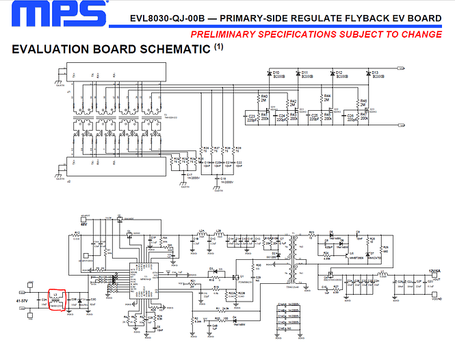
The first is about the inductor selection for VDD. It’s one common mode choke with the parameter shown below.
a. How do you decide on the selection of 1mH?
b. Is it because of EMI concern or voltage spike suppression? I guess this value depends on the schematics design as well.
c. If so, are there any methods or simulation tools that could be used to evaluate on our schematics design accordingly?
Manufacturer/model: WURTH/7448012501
Inductance: 1mH, Rated current: 2.5A, DC resistance: 55m ohm

The second question is about the current route for secondary side in terms of transformer, which is based on flyback topology. Could you provide the detailed explanation about how current goes in the secondary side of the transformer?

In case you couldn't see the attached image, the reference document is EVL8030-QJ-00B -- PRIMARY-SIDE REGULATE FLYBACK EV BOARD
Thanks for your time to spend on this consultation.
Warm regards,
Bill