Hi everyone,
I am debugging a PoE flyback design using the MP8017GL-Z in Primary-Side Regulation (PSR) mode and would appreciate any suggestions.
Design Summary
-
Controller: MP8017GL-Z
-
Topology: Active Clamp Flyback (PSR)
-
Input: IEEE 802.3af PoE
-
Input Voltage: 51 V from PoE switch
-
Expected Output: 12 V
-
Transformer: EP475SG-10
-
Bias winding: Not used (PSR configuration)
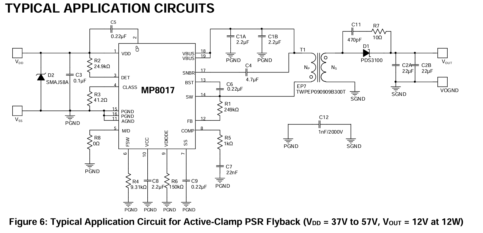
The design closely follows the MP8017 PSR reference schematic in the datasheet.
Problem
The PoE interface powers up correctly, but the flyback converter never starts switching.
The SW pin remains at approximately 52.7 V DC with no PWM activity (verified using an oscilloscope).
The output voltage is only 3.67 V after the output Schottky diode.
- Are there any common layout or component issues that can prevent the MP8017 from leaving startup in PSR mode?
- Has anyone successfully used the EP475SG-10 transformer with the MP8017?
Any suggestions or debugging ideas would be greatly appreciated.
Thank you!
A good place to start would be to check this with the typical application schematic. Does your schematic that you have match up with this? At the worst case, have you tried replacing the IC?
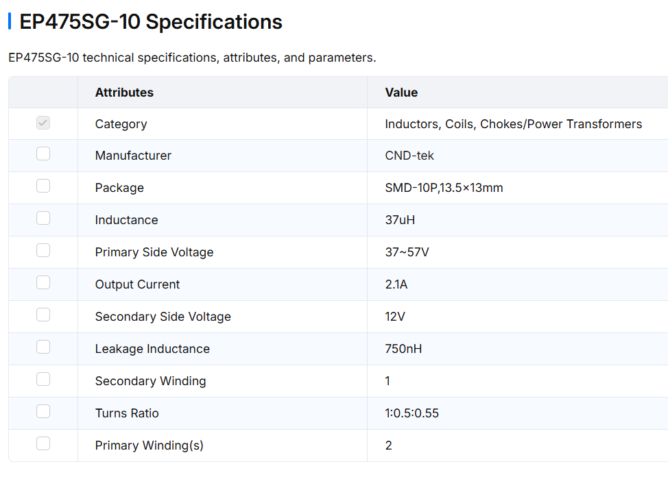
Also, what is your expected load? This is defined for a 12V @ 1A output. The transformer you have chosen seems to be fine, no issues according to the following specs (assuming your load doesn’t exceed 2.1A):
You mention that the SW node is ~52V. Is this waveform flat or is this seen as a square wave?
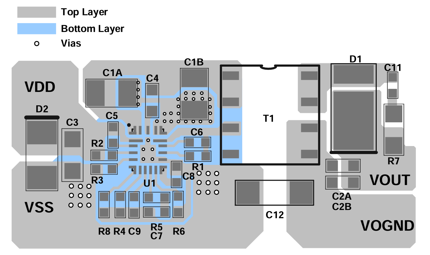
This is the layout as shown in the datasheet with the guidelines listed out below as well:
- Keep the input switching loop between the flyback input capacitor, transformer, SW pin, and PGND as short as possible.
2. Keep the output loop between the rectifier diode, output capacitor, and transformer as short as possible.
3. Keep the active clamp loop between the active clamp capacitor, transformer, SW pin, and SNBR pin as short as possible.
4. Keep the input hot-swap loop between the PD input capacitor, VDD pin, VBUS pin, and VBUS capacitor as short as possible.
5. Place the VCC capacitor close to the VCC pin for optimal decoupling.
6. Ensure that the feedback trace is short and routed far away from noisy sources, such as SW.
7. Keep other signal leads (e.g. DET, CLASS, COMP, VDIODE, SS, and FSW) as short as possible.
8. Shorten the CP loop and BST loop for excellent hot-swap and HS-FET driver function.
9. Use a single-point connection between power GND and signal GND.
10. Place copper and vias under the MP8017 package for excellent thermal sinking.
Hello,
Thank you for your suggestions.
I wanted to provide an update on this issue. It has now been resolved.
The schematic was based on the MP8017 PSR reference design, and the expected output was 12 V @ 1 A. The EP475SG-10 transformer was indeed suitable for the application.
After further debugging, we found that the root cause was a faulty MP8017 IC. Replacing the IC immediately restored normal operation, and the converter started switching as expected.
Thank you again for taking the time to review the issue and for your helpful suggestions. I appreciate the support.
No problem, I’m just glad that you found the issue by replacing the IC. Makes me wonder what went wrong here that affected operation.
Thank you! I really appreciate your time and the suggestions.
It was definitely an interesting one to debug.  After checking the startup sequence, verifying all the supply rails, bootstrap, feedback network, and comparing everything against the reference design, we were still seeing no switching. In the end, replacing the MP8017 immediately brought the converter to life, and the board has been operating normally ever since.
Unfortunately, we couldn’t determine exactly what caused the original IC to fail. It may have been a defective device or it could have been damaged during manufacturing or handling, but we don’t have enough evidence to say for certain.
We’re now continuing with full functional and validation testing, and so far everything is looking good.