Hello, I used the MP8008GZ-V reference design for our own board, it is almost the same, just minor Schematic changes about the auxilary power port, but it doesn’t work!
What am I doing wrong?
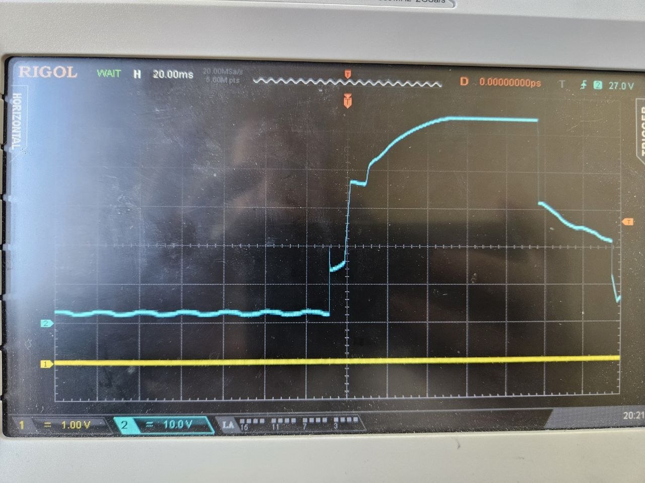
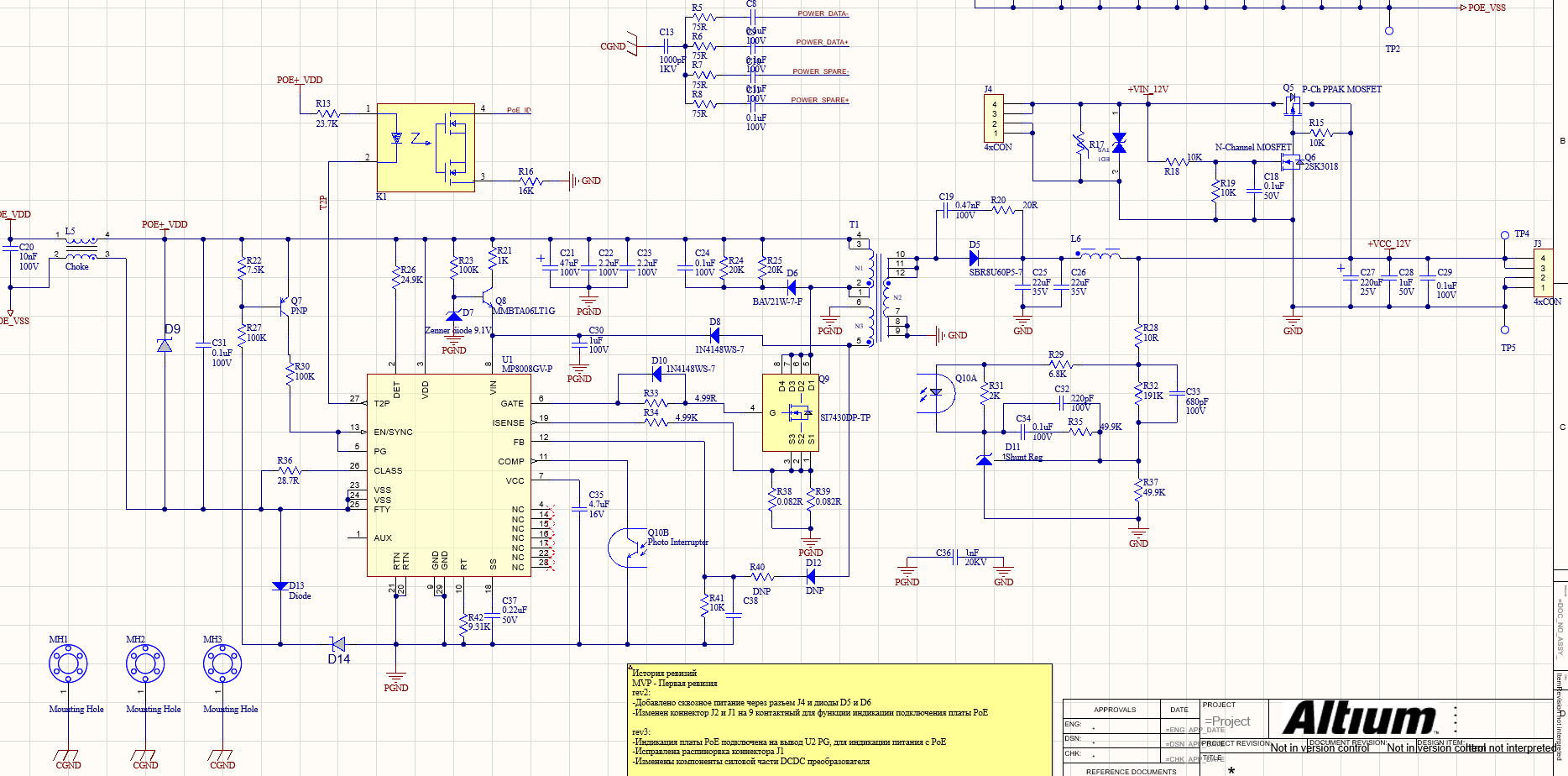
here is the schematic and VDD-VSS inrush oscilloscope diagram
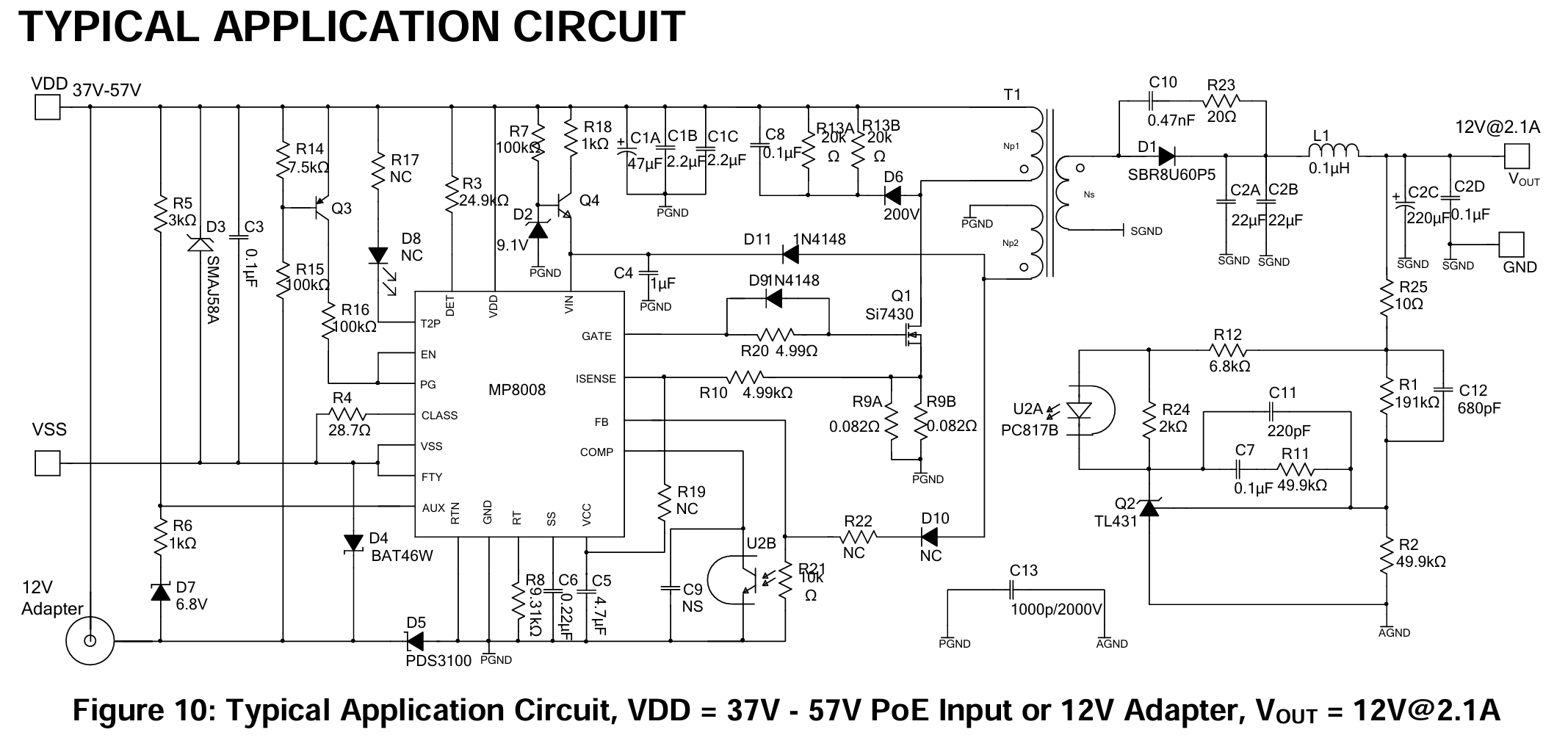
Is your design flexible enough to replicate this schematic? It looks as if you are mostly following this design minus the following:
It looks like you aren’t using the AUX pin despite this being an auxiliary power application. This pin functions as an auxiliary power input detector. This isn’t hindering performance, but I would recommend that this pin be used.
In the reference schematic, it would perhaps be best if you added a NS placeholder for C9 in case this is needed. Again, not a function killer, however this is always good to have for filtering noise and stability at the feedback.
I didn’t see any other striking differences between this schematic and the one that you have provided.
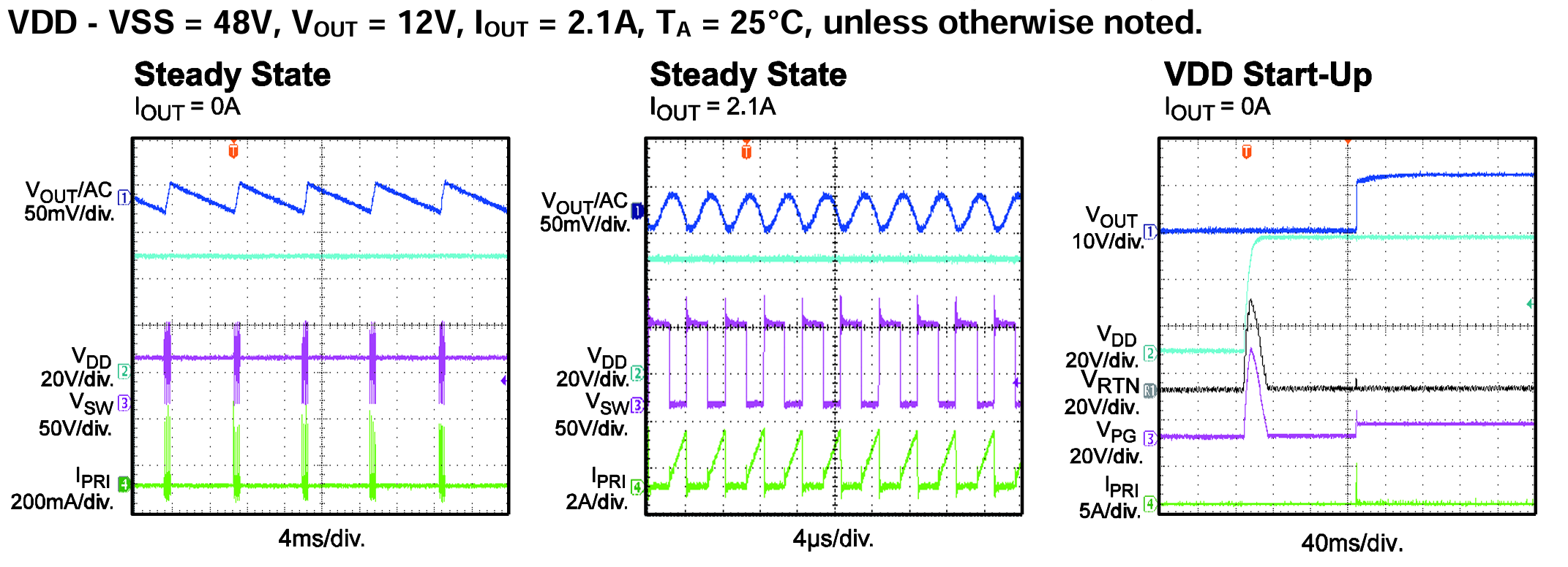
Can you replicate the following waveforms for further diagnosis at steady state during unloaded and loaded conditions?
What is your Vin, Vout, and Iout (I can only assume that this the same as the typical application based on the schematic, but I want to be sure)? Since VDD - VSS fluctuates as it does, what is your input supply?