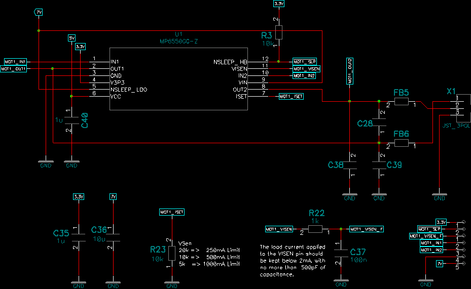
Hello, I created that ticket, because I have questions reagarding to MP6550 and I wasn’t able to find a lot about that IC resource center.
-
Is it expected to have a offset of ~40mV at I_sense ?
So, do I need to subtract 40mV in the uC’s ADC result ?
Evidence in the attachment. -
My uC has a DAC. Is it possible to connect the DAC → 2k → ISET ?
So, connect ISET with 2k to DAC instead to GND to have SW controllable current limit.
2k to DAC instead of GND
ILimit = 2.5A
U_Rlim = 2k/250uA = 0.5V
DAC 0.0V => ILim = 2.5A
DAC 0.1V => ILim = 2.0A
DAC 0.2V => ILim = 1.5A
DAC 0.3V => ILim = 1.0A
DAC 0.4V => ILim = 0.5A
DAC 0.5V => ILim = 0.0A
0.5V => ~620 DAC steps
=> 2.5A/620 = 4mA
-
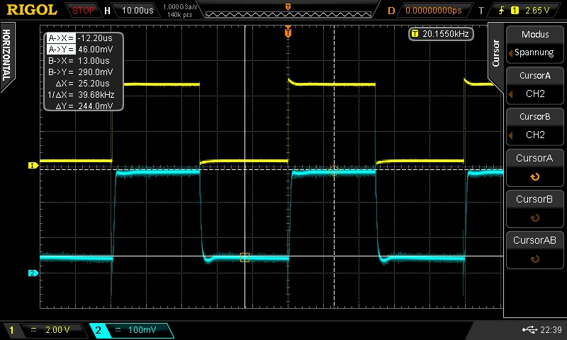
I connected a small motor (without load) to the IC. It wondered, because powering the motor with 50% PWM takes more power, then full power (100% PWM).
Is it right, that with 50% PWM, the motor is 50% accelerated and 50% slow decayed, takes more power, then 100%. -
An optional question. Why was it decided to have a “Current trip voltage” of 0.5V ? Then I loose a lot of resolution with the ADC. E.g. the MP6515 has 1.5V.
Attachment:
Measured with
- ISET 10k to GND => I_Limit = 500mA => V_Isen = 500mV @ 500mA
- C at V_Isen disconnected
- scoped directly at V_Isen
- only used resistor as load
- VCC = 4.8V, 20Khz, 50% PWM
- 33.00 Ohm => 145mA, expected V_Isen = 145mV, measured 166mV => DS2_QuickPrint1.bmp
- 16.50 Ohm => 291mA, expected V_Isen = 291mV, measured 290mV => DS2_QuickPrint2.bmp
- 11.00 Ohm => 436mA, expected V_Isen = 436mA, measured 410mV => DS2_QuickPrint3.bmp
- 8.25 Ohm => 582mA, expected V_Isen = over limit => DS2_QuickPrint4.bmp
[I wanted to attach some scope pictures and schematics here, but it was prohibited for new user.![]() ]
]