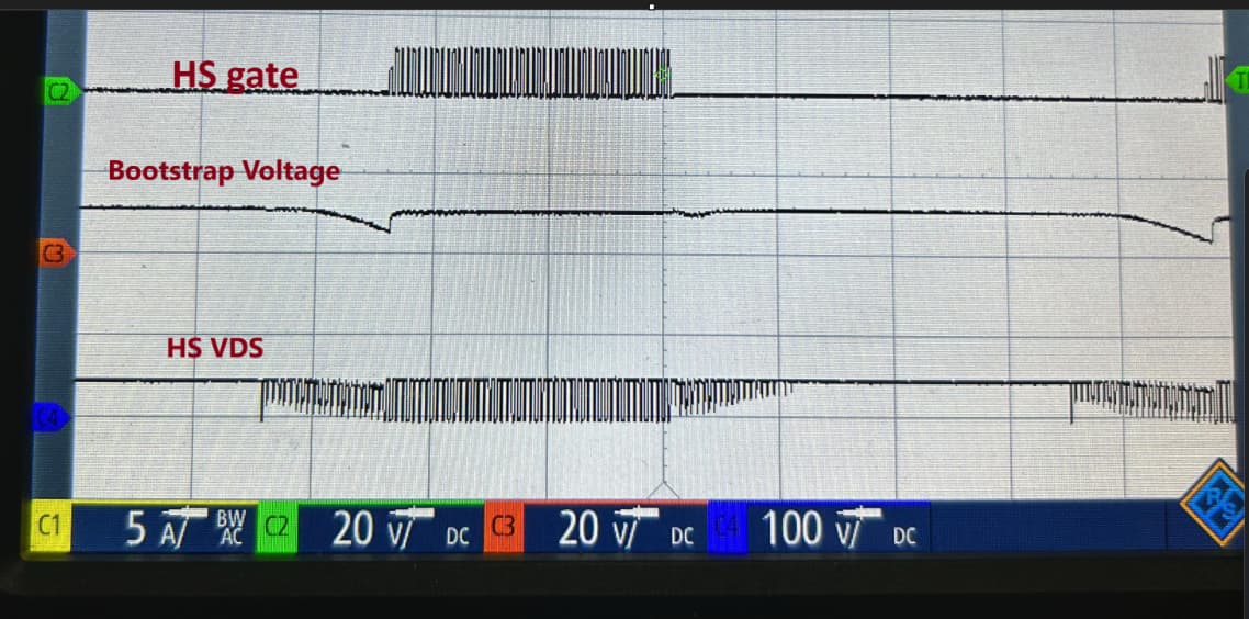
Hi I am using MP6539 for driving a BLDC motor using using six step trapezoidal control. The Gate Driver triggers a latched fault on nFault and shuts down as the speed of the motor increases (Note: We have not yet loaded the motor, only no load conditions). After a little bit of investigation and analysis of waveforms, we found that this happens because of a drop in Bootstrap voltage which appears not during the switching of the corresponding HS gate but just before the switching starts. During this time the source of the same HS FET is floating and sees the back emf from the motor. The BS voltage starts dropping as seen in the waveform and when the switching starts, the first gate pulse doesn’t get sufficient voltage to turn on the FET resulting in Vds staying High and thus triggers a latched fault due to High Side vds monitoring.
We want to understand why the bootstrap voltage is dropping and what can be done to rectify this. The BS capacitor placement is same as the reference design on your website.
Hi,
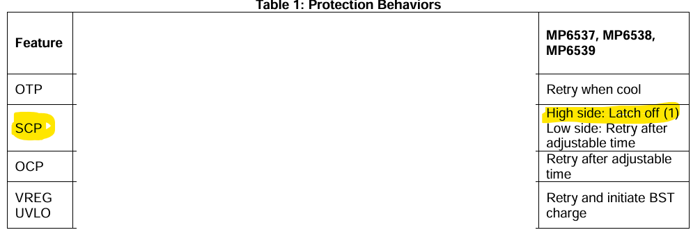
Welcome to the MPS Forum. Sorry to hear you are experiencing a shutdown with the MP6539. Thanks for providing the waveforms. nFault will latch whenever there is an Over Current (OCP) or Over Temperature (OTP). What current is needed to drive your external FETs?
For context, the bootstrap capacitor is charged whenever the LS-FET is turned on. If left on for too long, the bootstrap capacitor will slowly discharge (which is what I believe you are seeing). VBST UVLO (measured between SHx and BSTx) is ~4V. Once UVLO the part initializes a new power on sequence. Are you seeing this as well? What is the actual voltage seen at the minimum point for VBST?
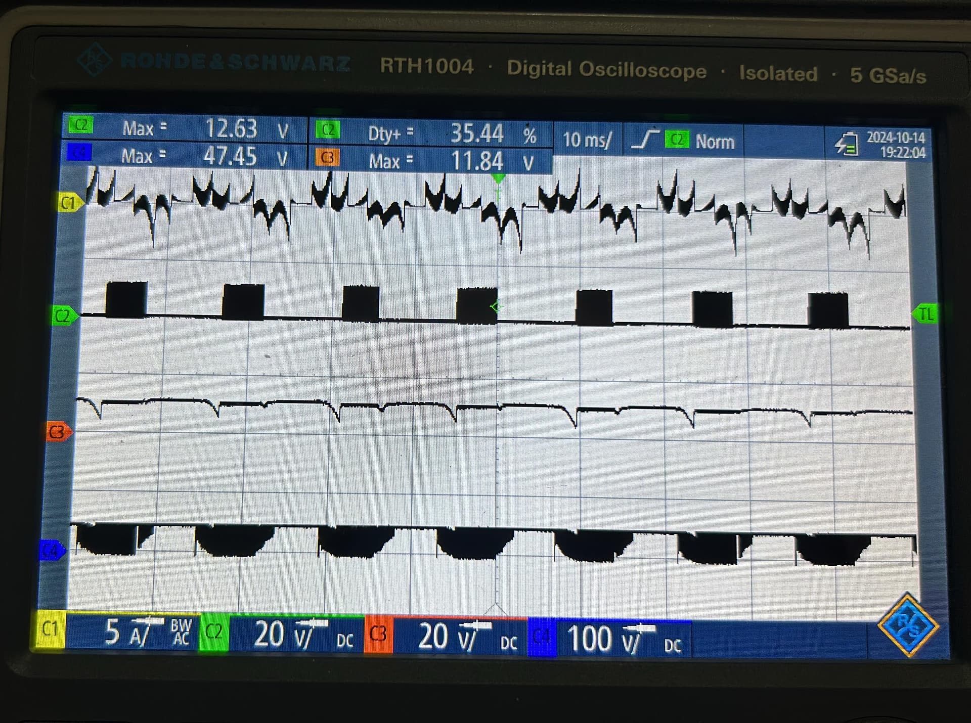
Could you provide a scope capture of when nFault is seen? Specifically, a capture including the LS-FET waveforms as well.
Could you also share your schematic?
Hi Stephan,
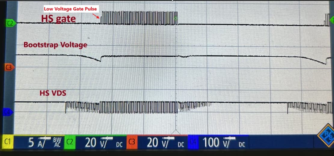
As I mentioned in the original post, the drop in VBST is not during turn on phase of the HS FET, it happens when the corresponding phase is left floating during the six step commutation as shown in the waveform shared earlier. VBST goes as low as around 3.9 volts (not accurate measurement) but my guess is that latched fault occurs not because of a VBST UVLO event since there is no new startup sequence happening, the IC stays in fault even after as well. The latched fault occurs due to the lower Gate Voltage for the HS FET when the drop in VBST is observed, which triggers the SCP for High side resulting in a latched fault.( Screenshot from Application Note for MP6539)
It can be seen that the gate voltage for the first pulse is at a lower voltage due to the drop in VBST, which results in an incomplete turn on of the HS FET resulting in the SCP trigger for High side.
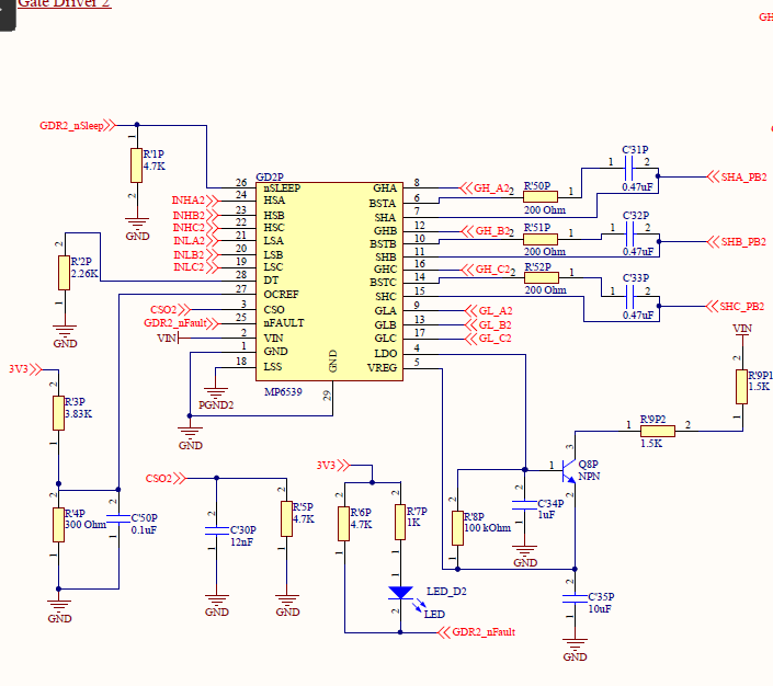
In the Schematic, there is a mistake in the value of the bootstrap resistors R50, R51, R52, The values used in the test board is 0ohms.
Thank you for clarifying. I can agree, the latch can be due to SCP. There are a few ways to address the latching you are seeing.
Since the HS FET does not turn on fully which triggers the fault (as you stated), you can try to increase the BST capacitor rating which will provide more current so you will get a full turn on at the HS gate (use 0.68uF to 1uF). Additionally, SCP can be triggered if the rise/fall time is less than the blanking time. In other words, the FET should be fully turned on by the time the deglitch/blanking time has finished.
Vreg/LDO capacitor should be higher, recommended 10uF. Too low of a capacitor can also trigger SCP.
If this does not resolve your issue, please feel free to contact MPS and we can work with you directly.
Contact MPS - Contact (monolithicpower.com)
Hope this helps!
1 Like
Hi Stephan, my main question is not why the nfault is triggered, that part is clear as I have reiterated in my previous comments. My question is why the bootstrap is discharging and a drop in voltage is seen, what is the discharge path, because when the drop appears neither the HS FET nor the LS FET is on, then where will bootstrap discharge into. This indicates that the bootstrap capacitance is discharging through the IC somewhere. Can you figure out the discharge path? Also do you have some waveforms for the bootstrap voltage for your reference designs (120 degree /six step commutation)? This will help understand the issue.
Hi Anshu,
Speaking with one of our application engineers I have gotten a bit more information. There is an internal leakage path within this IC. The path is connected to SHx, VDS sense, and the gate driver. This can be seen in our functional block diagram on page 10 of the datasheet. The voltage drop seen by the VBST is due to the required discharging to provide enough charge to turn on the HS FET before a complete turn on. This is expected when neither the HS or LS FET are on, i.e before the corresponding phase is turned on.
We do not have any waveforms for the bootstrap voltage for our reference design.
So what is your suggestion to fix or improve this behaviour?
To make sure the VBST doesn’t dip below the VBST UVLO and trigger an SCP fault you can increase to 1uF. It is also possible to increase further but, 1uF is recommended.