Hi MPS team,
We are working with the Fab house and encountered an issue with the soldermask and pastemask of the footprint, which were built based on the recommended footprint in the datasheet.
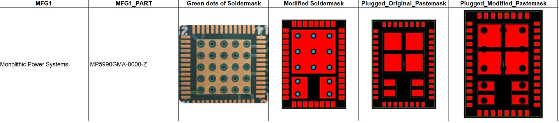
Currently, We apply Non-VIPPO for this design. Therefore, all the via will be plugged with solder mask including vias on FET SMD pads.
The picture below shows some green dots of soldermask (please see on the table) , and it would be placed on top of SMD pads.
We have modified the soldermask of the FETs to fit via plugging treatment. However, with the pastemask design, we are confusing between 2 options:
-
OP1: Keeping the pastemask as recommended in the datasheet will lead to solder being blocked by the soldermask of the vias (green dots in the picture above), due to reducing the pastemask ratio and it maybe cause thermal issues.
-
OP2: Modifying pastemask to avoid soldermask of the vias and improve pastemask ratio.
Please see table below for details.
We have 2 databases with different pastemask design:
-
Plugged_Original_Pastemask: FETs are designed with Modified soldermask for Plugged via and Original paste mask as manufacturer’s recommendation.
-
Plugged_Modified_Pastemask: FETs are designed with Modified soldermask for Plugged via and Modified paste mask to void soldermask dots and improve pastemask ratio.
Could you help to review and give us an advice if there are any issues or potential risks.