On this PMIC MP5470BGL-0000, I have a few questions.
-
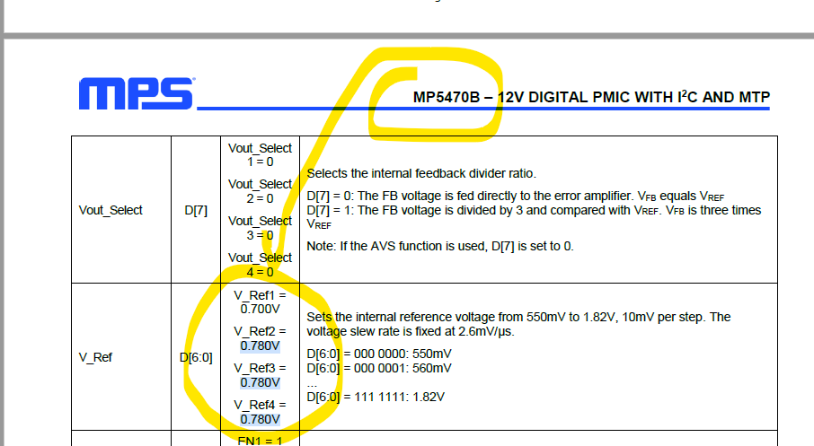
Are the default voltages for this device always factory set at Vref1 = 0.7 V while Vref2=Vref3=Vref4 = 0.78V. This means the designer has to carefully select the correct feedback resistors based off these voltage values.
Otherwise, during first time power up, if the designer assumed Vref = 0.55V, accidentally driving the enable pin would turn on the regulators and cause an overvoltage condition on the load devices.
-
It looks like the designer has to first disable the Enable pin before writing the I2C registers to change the voltages to the desired value.
-
Can unused SW4 and FB4 be left floating? Or should they terminated in a certain way or shorted together?
-
If the I2C/MTP register enable is set to disable, does the external pin override it? Or do both need to be set to enable to turn on the regulators? Likewise, does the external enable PIN have override the regulator. Say I2C register is enabled but pin is set to disable, does the regulator get disabled?
Thank you.
Hi Frank,
Thank you for posting on the MPS Technical Forum.
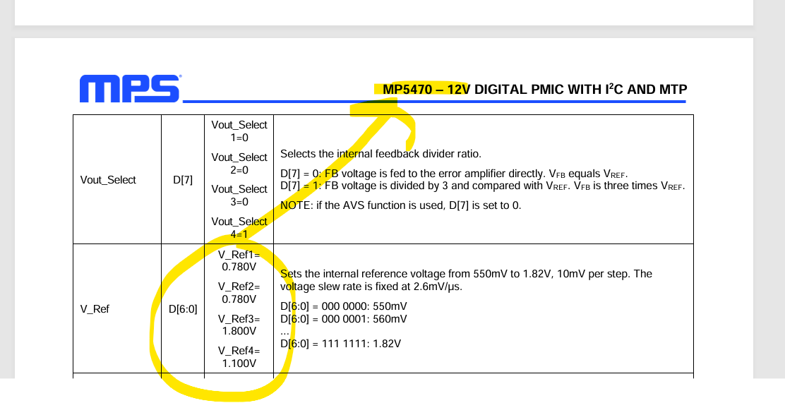
- Default reference voltages read: Vref1 = 0.78V, Vref2 = 0.78V, Vref3 = 1.8V, Vref4 = 1.1V. This is the default version of the part (-0000), and should be taken into consideration when first turning on the device.
- Best practice would be to follow the timing diagram in Figure 5 of the datasheet. Note that VCC needs to be pulled up to 2V when writing to MTP.
- Yes, if buck 4 is not used, leave SW4 and FB4 floating. I would suggest disabling buck 4 through bits D[7:4] since its default is enabled.
- The EN/SYNC pin will turn on/off any buck outputs that are configured as “on” in I2C. If the I2C/register is set to disable, the physical pin shouldn’t be able to turn it on.
Let me know if anything is unclear or if you have other questions.
Thanks,
Allison
Hi Allison. Thanks for the reply.
The datasheet for the MP5470B shows this Vref1 = 0.7 V while Vref2=Vref3=Vref4 = 0.78V.
I think you responded with the values for MP5470 without the “B”
See both versions below:
Hi Frank,
Ah yes, I did. Thanks for catching that.
I believe my other answers should remain the same. The “B” version changes those values and included an update to the MTP.
Best,
Allison