Hi,
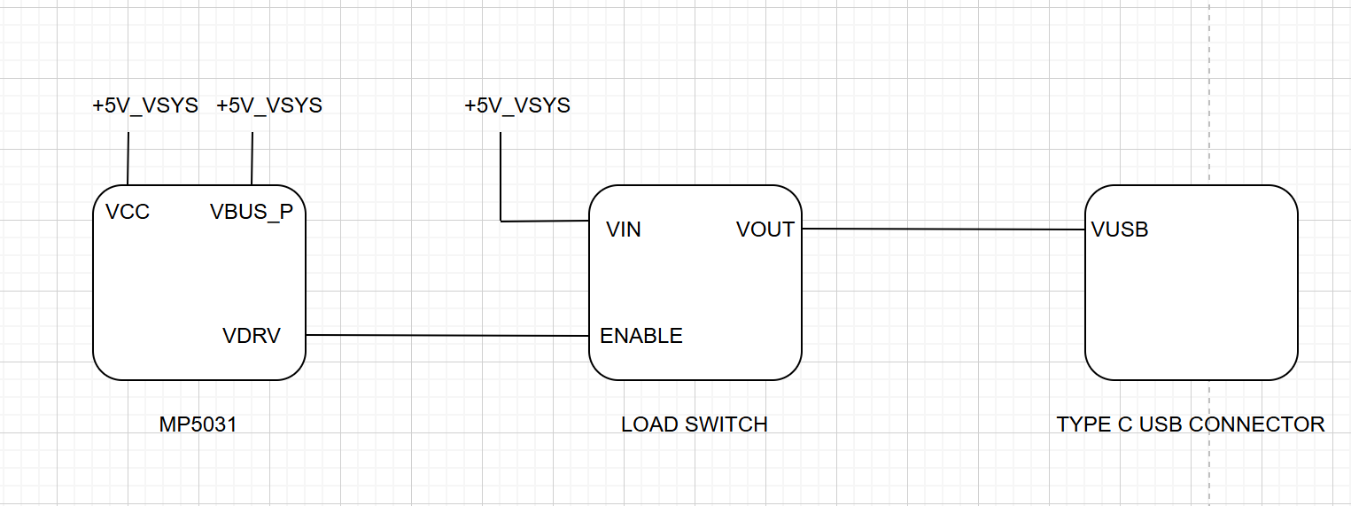
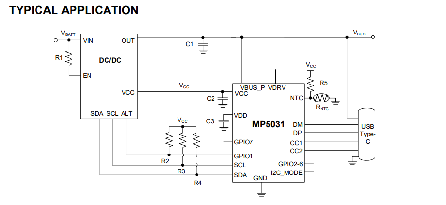
I’m planning to create a circuit as shown in the attached image. In the reference circuits for the MP5031, I’ve noticed that a buck-boost converter is typically used. However, in my design, I intend to use a step-down converter to provide a 5V output that powers both the USB Type-C port and the MP5031.
To prevent current backflow and manage inrush current, I’ve incorporated a load switch between the 5V source and the Type-C connector. The VDRV pin of the MP5031 will drive this load switch. When a USB device with a battery is plugged into the USB port, the MP5031 will enable the load switch and manage the PD (Power Delivery) negotiations.
My questions are:
- Is there any issue with this design approach?
- Where should I connect the VBUS_P pin of the MP5031—before or after the load switch? Since the VBUS_P pin has a discharge function, and I’m connecting it to the 5V system power, I want to prevent any unwanted discharge. How should I handle this?
Thanks