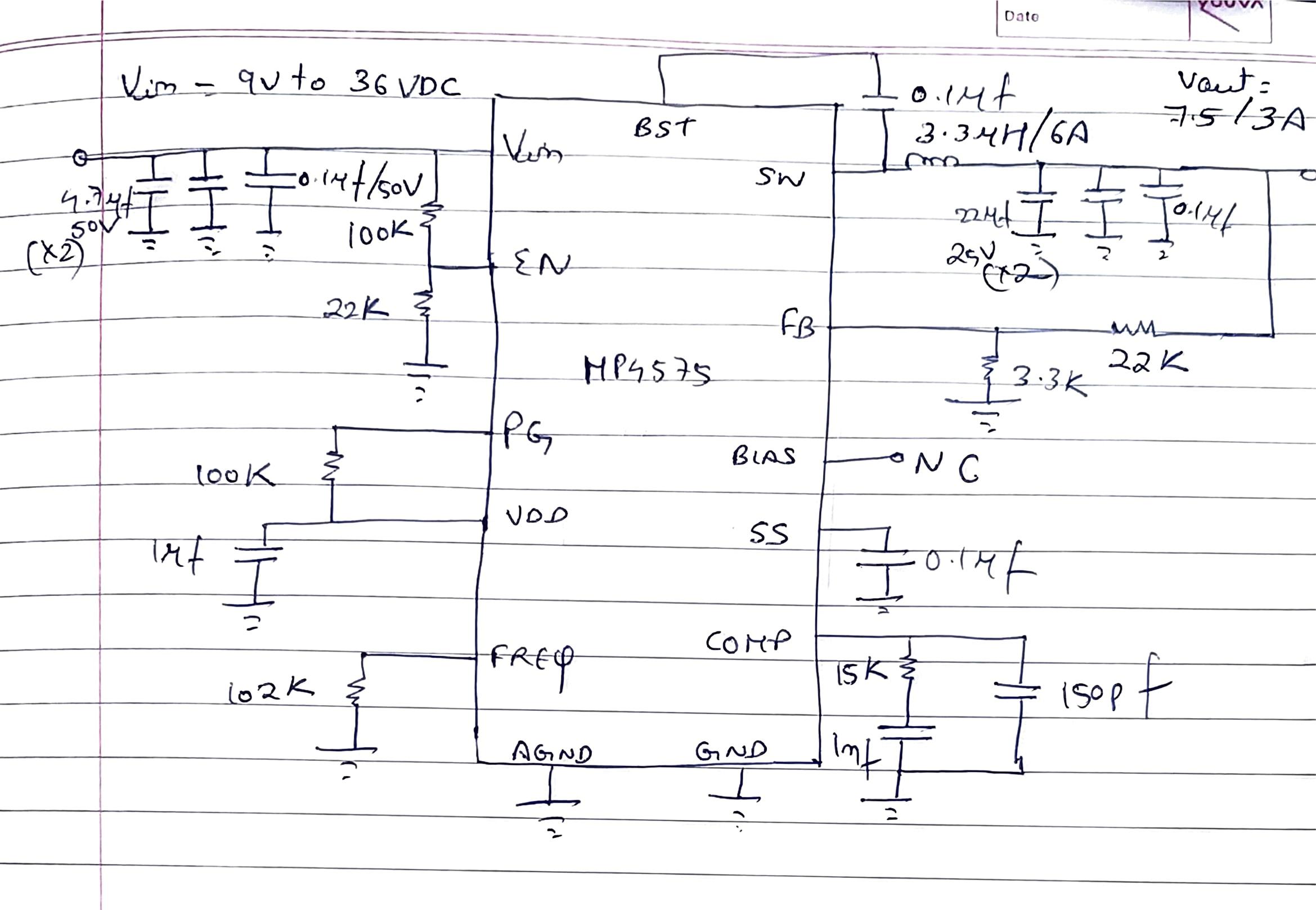
Since you are concerned about the output ripple, you can increase Cout to 2x 47uF instead of 22uF.
For your comp network, with a 15k Rcomp, set C3 from Rcomp to GND somewhere > 2nF. The value of C4 in parallel with Rcomp and C3 depends on the ESR of your output caps.
EN should be pulled high or low, so you should probably depopulate the 22k Rdown. You can connect EN to some additional circuitry to pull the pin down to disable it if necessary.
I think the rest of the application looks fine. If the duty cycle is consistently high and you’re operating on the lower end of your Vin range, you might consider a BST diode as well.
I have concerns, regarding BST diode as there might be a case, where we will be operating at lower VIN range as input source is a battery which will drop to lower side of input voltage range i.e 9VDC.
Since input voltage range to BST pin is 3V-5V rail and this entire dc-dc module is a standalone circuit in our design we do not have external voltage source of 3-5VDC to apply at BST via diode as output is set to 7.5VDC.
What will be the case at VOUT here in absence of BST diode during higher duty cycle ??
I’m Braian Bannert, the R&D Manager of an Argentinian company.
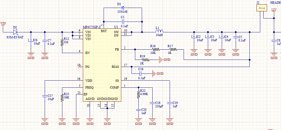
I’m responsible for designing new devices in the company and now I’m designing a device that has embedded the MP4575GF-Z IC. I designed the power supply to have an output of 12V/5A with an input voltage that could be 12V or 24V and when I power the input power supply I get an output voltage of 0.3V. Please see attached the configuration made for this power supply mentioned before.
I need to mention that I noticed the diode D1 was not properly connected. I made the changes needed to connect it to BST pin and the track of the output of the power supply (12V in this case).
Please let me know if there is something I made a bad calculation or connection to be improved.
For this request, please fill out the MPS NOW Technical Support form. A member from the MPS NOW team will contact you within 24–36 hours about this request.