I’ve got a circuit using the TSOT MP3437, following the schematic and inductor selection from the online design tools. 3V-4.2V in, 12V out @ 1A. It seems to run fine under minimal load, but when put it under any real load, it appears that the converter just starts switching itself on and off.
This in with the boost circuit in isolation, supplied off a bench supply, into a purely resistive load.
Interestingly, if I increase the supply voltage up past 5V, the issue seems to go away.
I’ve followed the example circuit exactly, and the inductor I’ve chosen should be fine. Calculator said the peak current would 4.5A, and the inductor is rated for a peak of 6A, with a saturation of 7A.
The above scope printout shows the output switching from no load, to around 0.5A.
Hi Sbitney,
Is 1A the minimum load value where it is working fine based on your Vin values? What is the resistive load value set at it starts switching?
Regards,
Adhish
Hi Adhish,
It turns out that my testing setup had an issue. The bench supply had a lower current limit set, as I wasn’t expecting much more than 1A draw during testing, based on the expected approx 90% efficiency. It was the bench supply overcurrent that was causing that switching behavior.
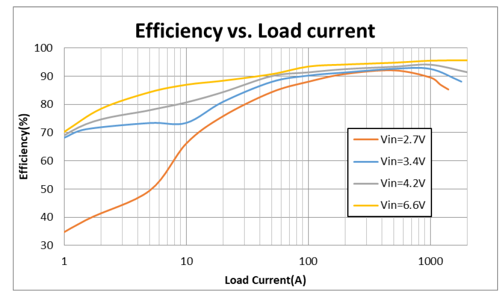
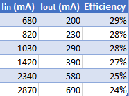
What is happening is the efficiency is actually very bad. Between 0.2A and 0.7A, I’m measuring an efficiency of 30% to 25%, and if a load was left applied, the efficiency becomes even worse, I assume as the driver starts to overheat.
But I’ve got no idea what would be causing it.
Even selecting the inductor we’re using (Wurth 78438357033) into your circuit designer, we should be expecting an efficiency of around 91% under load.
Hi sbitney,
Good to know, that the switching issue has been taken care of.
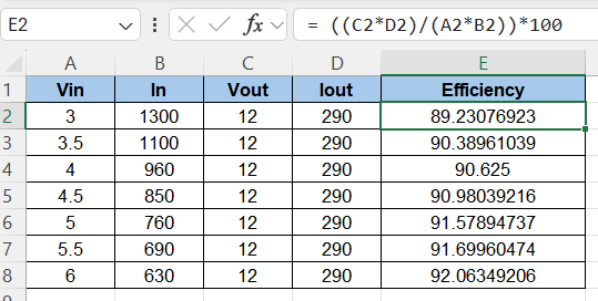
Regarding the efficiency values, it depends on the Vin and Vout value as well not just the current values. From the values that you have attached looks just the division of Io/Iin, which does not look right to me.
Did you try checking the efficiency at different input voltages keeping the load constant(for eg 1A) once and then gradually decreasing/increasing load current keeping the Vin constant?
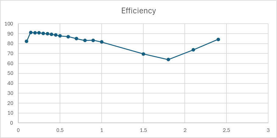
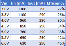
I did check from my end it shows the following efficiency when Vout =12, load from 0A~1.5A
Additionally from your schematic, the EN pin is getting a digital signal I believe, as per our datasheet it is highly recommend to pull up or pull down.
If this also does not works, then changing the inductor can be one way to think off as due to some reasons such as layout, etc. it might be having higher input losses overall due to which the efficiency is going down overall.
Regards,
Adhish
Previous testing was done with a constant Vin of around 3.7V.
I’ve done some further testing with a fixed load and a varied Vin, and the efficiency does increase with Vin as expected, it is still far below what it should be.
The losses seem to be in the chip itself, rather than the inductor, as the chips get very hot during testing, and we’ve had a couple die in testing, presumably due to the thermal stress.
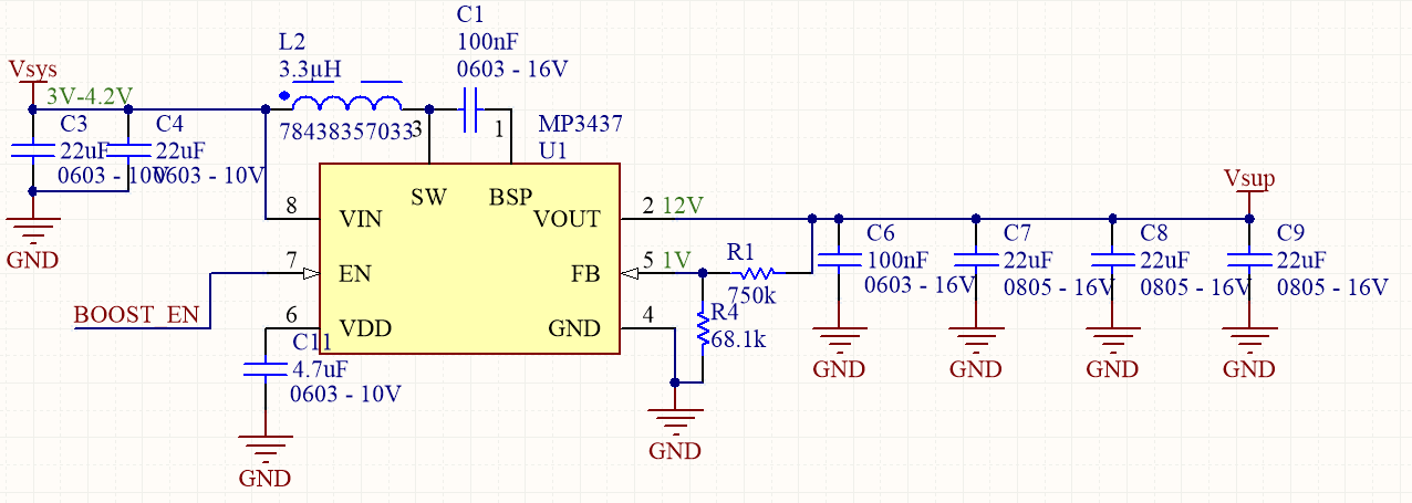
As for the enable line, it is normally controlled by a open collector output and a 100k pullup, allowing us to disable to supply when not needed, but for testing, I’ve just got the pin permanently pulled up to Vin using a 10k resistor instead.
Here’s Vsw for Vin 6V, 5V and 4V. Other than the second pulse on the 6V Vin waveform, they look how I’d expect.
1 Like
Also, just tried it with a much larger inductor. Still 3.3µH, but 14A 8mΩ rated one, instead of 5A 33mΩ, and I’m getting around the same 30% efficiency at 4V Vin, 290mA Iout.
Hi sbitney,
Looking at the data you collected, it looks right to me, within the Vin range and at a constant load, 12V boost output is seen. The waveforms looks good as well.
I believe you are calculating the efficiency column somewhat wrong. I did a quick analysis on the points you captured at 290mA load and this matches as per our datasheet.
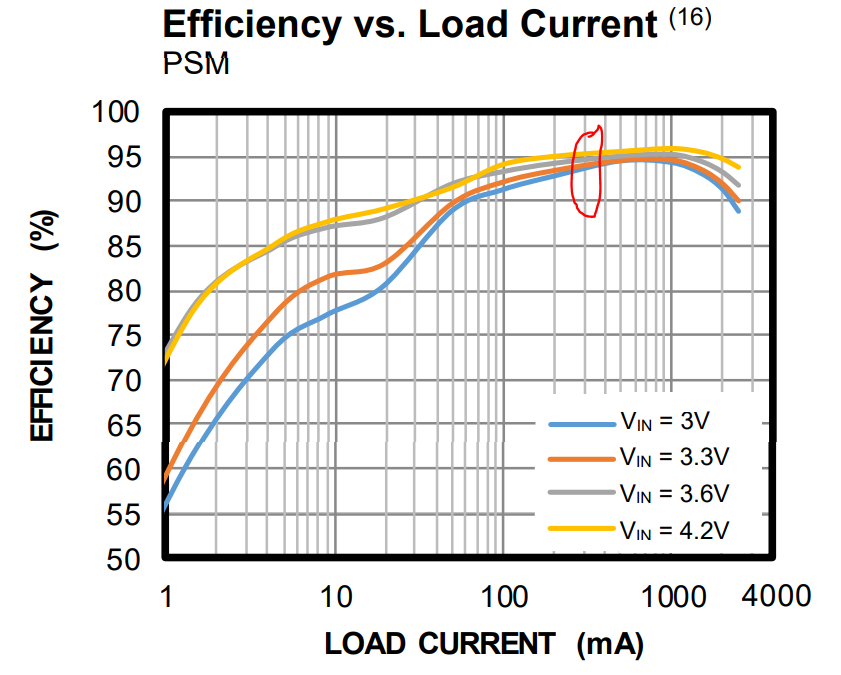
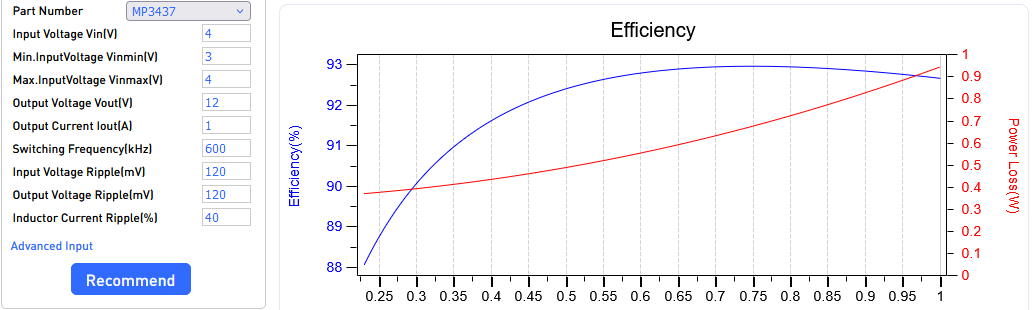
Also if you take a look at the datasheet for the Efficiency curve as shown below, it works as expected.
Secondly, what is the temperature at the chip you are observing when it gets hot?
“Couple of them die” do you mean it stopped switching at all?
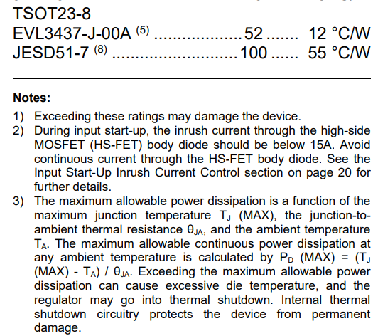
Just FYI, this IC has an internal over-temperature protection feature where it stops switching when it goes beyond 150 degree celcius.
In this case, I can suggest you some thermal dissipation calculations such as shown below so that you will be able to know how much power is getting dissipated and then doing necessary changes on your layout can be the next step.
Let me know if you have any more questions.
Regards,
Adhish
Hi Adhish,
Thanks for pointing that out. Of course those efficiency numbers didn’t make any sense, I don’t know what I was thinking.
However, redoing them correctly, it’s still showing numbers much lower than expected.
According to your circuit design tool, we should be just below 1W power dissipation at 1A Iout, which is within the 1.25W maximum dissipation figure in the data sheet, and assuming 100°C/W thermals, we’d be looking at 100°C above ambient, which should be within TJmax. We also don’t plan on running at 1A consistently.
However we seem to be hitting that 1W dissipation at a much lower output of only around 0.43A.
I’ve redone the tests with the much larger inductor, and the results are very similar.
I’ve checked the voltage at Vin and there’s no voltage drop between the input on the board and the Vin pin, so the loss isnt happening elsewhere on the board. Also, the chip is the only thing that appears to be getting hot.
I haven’t measured exact temperatures yet, I will do that tomorrow once I get access to a thermal camera.
As for the chips I’ve had die. After extended testing, where the chip gets very hot, I’ve come back the next day and there’s been dead shorts from Vin to GND. I’ve swapped the chips out with spares, and everything is fine. This has happened twice.
Hi sbitney,
Apologies for the delay in the response.
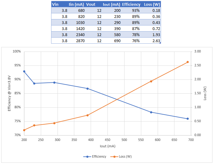
I went ahead and checked on our evaluation board with varied load current values keeping Vin=3.8V & Vout =12V, and I saw a trend when the load current is from 0.3A till 1A, the loop is getting unstable due to which the efficiency is getting low. See the below graph, which is your case as well.
In short, the phase margin is very less at this point for the converter.
In this case, I believe two things can be done to have better efficiency such as follows:
-
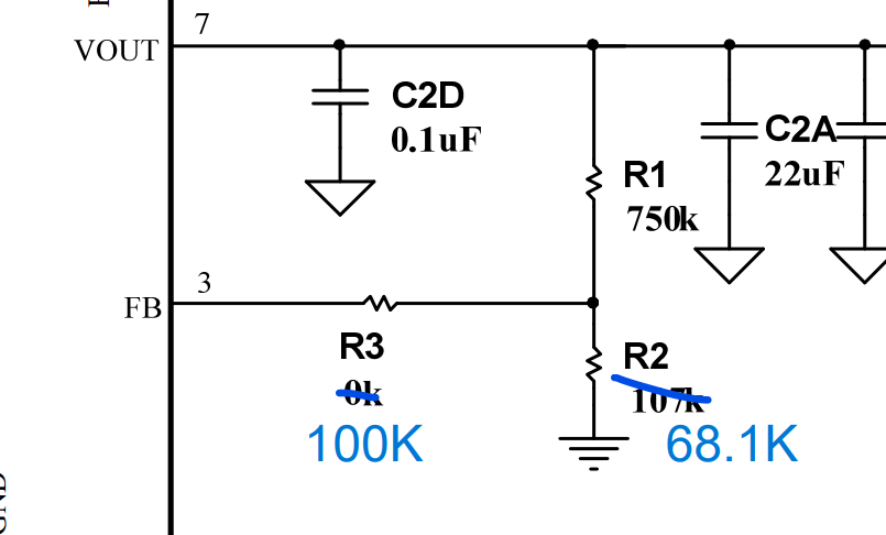
Add a resistor as R3(100k) to FB, so that it can improve the loop margin.
-
If there is no place to add a resistor, add more output capacitor or use 1210/25V/22uF cap.
Let me know if that works and if you can see an increase in the efficiency at higher load currents.
Regards,
Adhish