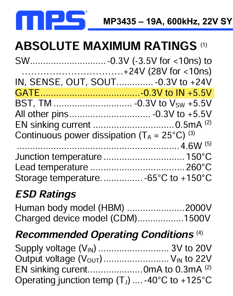
We are using the device for following in/out specification:
- Vin = 10V
- Vout = 13.5V
- Iout ca. 1-1.5A
We are using the design with external current sense resistor and disconnect MOSFET. We have used in our design a Mosfet with 2-4V Vgs threshold (e.g. BSZ440N10 from Infineon). According datasheet page 20 below figure 4 a Vgsth value below 1.5V is required:
“Gate-to-source threshold voltage: The
threshold should be below 1.5V. A 1V to
1.2V range across the overall temperature
range is recommended.“
The internal charge pump seems to be able to boost the Gate ~4.4V above the input voltage (~10V). The voltage drop across the Mosfet is ca. 60-70mV at ca. 0.6A load current, which is basically fine.
Q1: Can we stick with higher Gate source threshold voltages or what would be negative impacts?
Remark: There seems to be different OCP modes according table 3, which implies that for current limit during power up Vgate < Vin+1.6V
Q2: What is the maximum Gate output voltage above input voltage the internal charge pump can generate?
Remark: Actually we have measured \~4.4V but not sure if this can be guaranteed over the complete temperature range.
Thanks in advance!
BR Andreas N.
Hello Andreas, apologies for the delayed response.
Thanks for providing some background on your application with the external FET with the MP3435. For context, our evaluation board uses the SiS612EDNT-T1-GE3 (20V, 3.2mΩ, 19A N-channel MOSFET).
The BSZ440N10 that you are using has the following specs (100V, 44mΩ, 18A N-channel MOSFET). The voltage and current specs here are perfectly fine. If anything, maybe it would be worthwhile to go down on the RDSon to increase efficiency if that is a concern.
To answer your questions directly:
-
There should be no issue, the higher gate to source threshold just means you have loads of headroom.
-
This question would be answered by looking at the absolute maximum thresholds as shown:
Vgate >= Vin + 5.5V.
Hope this provided some insight. Let me know if you have any follow up questions.
Best,
Krishan
Hello Krishan, many thanks to your response. I’m a bit astonished about the answers.
Q1 related: So basically with much higher Vgs threshold than recommended the work modes according table 1 could not be achieved, e.g. linear charge mode, since the MOSFET with higher Vgs threshold will be simply OFF.
Q2: Can you confirm that the charge pump is really able to generate upto 5.5V? I read this only as maximum rating that the gate voltage must not exceed Vin +5.5V. It would be interesting if the internal charge pump is really able to drive at least 5V
Now I have selected other MOSFETs with lower Vgs threshold (1.5V max) as replacement for BSZ440N10.
-
FDMC8651 (ONsemi), VDS=30V, VGS=+/-12V
-
SiSH106DN (Vishay), VDS=20V, VGS=+/-12V
Unfortunately the MOsfets with sub-logic level in PPAK33 package are rare. So, personally types with max Vgs threshold of 2.5V max are more widely available and they have higher Vgs rating of +/-20V. So basically if the MP3435 design complies also with those MOSFET types this would be the better solution for us. However, this is not inline with datasheet table 1 and selection recommendations. Any advice would be helpful.
Thanks in advance!
Best regards Andreas
Excellent point on the Vgs threshold, thanks for the reminder via Q1.
As for Q2, this is indeed a maximum rating. I am unsure if the charge pump can actually go to 5V, but I hope from what you have observed for 4.4V, I’m hoping this should be good enough. Just ensure this does not exceed 5.5V above Vin.