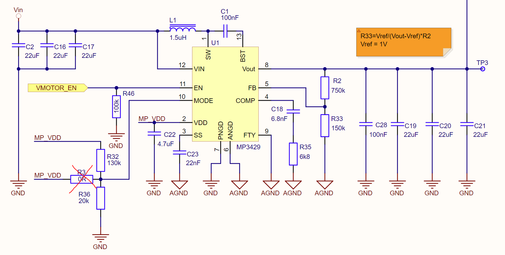
I am using a MP3429 for a project and keep having problems with it. I need a 6V @ 1.8A output and I believe that using this scematic and resistor values I should be able to do that.
I want to supply this schematic with 3V (should be possible if I am not mistaken). When doing that I can’t draw a current of the requested 1.8A. The output voltage on a multimeter drops to around 3.4V and the current doesn’t go anywhere near what I want. When connecting the output to a scope I see a ripple current of around 900mVpp. at a frequency of 67.6kHz.
I am not sure where to look for the solution. Can anyone help me?
Hi g.devries,
Is your PGND tied to AGND?
Where are you measuring VIn from? Is it from the input caps or somewhere further upstream?
What is the saturation rating of your inductor?
We also have a SIMPLIS model for it on: https://www.monolithicpower.com/en/design-tools/design-tools/mpsmart.html.
Regards,
Vinh Tran
Goodmorning,
Thanks for the fast reply. PGND and AGND are tied op the PCB as per the reference design. Vin is a wide trace running for 17mm. Also here I used the reference design as much as possible.
For L1 I used the104CDMCCDS-1R5MC. This one is also used on the development board. The saturation current of that one is 24A.
I will have a look at the tool.
Best regards,
Gido
Hi g.devries,
Could you check if your input supply is current limited? Since this a boost device, the input required will be greater than the output. The power supply maybe having issues with output current.
Are you also measuring this directly from the input caps / pins of the device? Or is 3V from the power supply? The higher current draw may be causing the wires to see a large voltage drop.
If you have SW node waveforms for good and bad operation, that would be helpful.
Regards,
Vinh Tran
Hello Vinh,
My apologies for the late reply. I was on holiday. The power supply is not limited in this case. I’ve also tried with a power supply capable of putting out 40A. Unfortunately to no avail.
I am measuring at the input caps.
I’ve managed to get you some screenshots of my scope. The naming of the files should be explanatory.
Test MP3429
Thank you.
Best regards,
Gido de Vries
Hi Gido de Vries,
Thank you for sending over those waveforms. There definitely is something not right as you reach the higher current levels. You would expect the waveform to look like the 1500mA sw waveform. However, it shows characteristics of DCM and looks like the SW node is unable to immediately rise up.
Could you check if the Cbst is damaged in any way? What is the voltage rating of the Cbst? If the Cbst is damaged the part is unable to charge the HS FET properly.
How are you measuring the SW node? Is it with a passive probe? Active? The SW node peaks look very high and maybe due to the measuring method. I am not worried about the overshoot, but if the undershoot is low enough it can damage the device. A way to mitigate this would be to add a Rbst, but that I would not recommend it yet. Please check the BST circuit first.
If it is also possible, could you send a waveform with the Vout at ripple at the same conditions of 3Vin 1700mA?
Regards,
Vinh Tran
Hi Vinh,
I’ve checked and tested Cbst and it has no damage. Neither visual nor electrical. The voltage rating is 25V.
I am measuring all the nodes on the scope with passive probes. I have 5 prototypes of my PCB of which a few have died testing the supply.
I’ve added a few screenshots to the previous supplied link.
In addition to this, I’ve taken the liberty to buy the development board of this component and changed the R2 value to configure the output to 6V. I’ve done the same measurements with this board and this board (obviously) works like a charm.
Best regards,
Gido de Vries
Hello Vinh,
Have you had time yet to take a look at the added figures?
Best regards,
Gido
During my research I’ve found that the in- and output capacitors I used were 0603 SMD’s whilst the caps on the development board were 1210. The only difference being size and voltage rating (10V vs 25V). At the time I thought 10V would be enough since I was only converting 3V to 6V. Turns out, with the 1210 caps from the dev kit, my PCB works.
Now to reduce the spikes on the output voltage. On the switching flanks the ouput voltage has spikes up to 600mV above and below the set voltage.