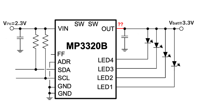
We are considering the MP3320B as driver for the RGB signal LED on an IoT sensor. We have two voltage rails:
- Vi2c=2.3V which powers all I²C devices on the sensor
- Vbat=3.3V which powers devices that need a higher operating voltage.
It must be possible to have Vbat=0V with Vi2c=2.3V as well as Vi2c=0V with Vbat=3.3V. In other words, we have to be able to set one of the voltage rails to zero without extra current leak.
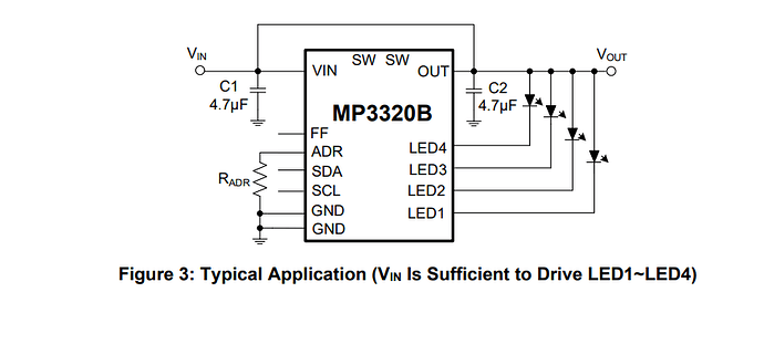
Based on Figure 3 of the datasheet we want to operate it like this:
The questions we have are:
- Is this setup possible at all?
- Should we connect Vbat to OUT or rather not?
- Will it be possible to have either Vi2c or Vbat to be 0V? Or are internal (parasitic) diodes prohibiting this?
- Will a toggle on Vin (Vi2c in this case, which also takes the SDA/SCL down) indeed reset the internal I²C state machine of the MP3320B?
Thank you for any guidance, best regards, Ruud.
Hello,
Can you share a bit more about your system? You will have the output connected to a battery? What functionality are you looking for? Keeping the LEDs lit?
Hi Eduardo,
Thank you for your time to look into my case. To answer your questions:
- Vbat is not a directly connected to a battery but is from a buck-boost converter which keeps the voltage on 3.3V (as long as the battery supplies the power of course) for sensors that require a voltage of that level. If none of the devices need the supply it is switched off.
- Vi2c is derived from a microcontroller and can be toggled if needed to reset the bus if one of the devices on the I²C hangs. Or, if we do need to take measurements for a while, we may switch this off.
- The functionality we need is rather basic, no full blown light shows, but merely a quick flash one, two or three times, in one (maybe mixed) color at the time. This is to report the internal state, primarily during configuration. During operation the LED will flash green (a short as possible) once every few minutes to indicate the node is operating well. If the battery gets tight, this color must change to red.
So we basically utilising this chip to save I/O lines and as set of current sources, but mostly because it offers all this on very little area. PCB area is very, very limited. We do not want to use the internal boost to draw from the Vi2c, for we fear surges on that line could interfere with other sensitive sensor chips.
I hope this helps you to answer my four questions. Thank you again.
Best, Ruud.
Hello,
I believe that a voltage must be applied to VIN the MP3320B for operation. The following does show a scenario where the internal boost is not utilized but it does have the input voltage going into VIN pin and then also connected to the LEDs. I do not believe having Vi2c = 0V would allow for maintaining functionality of LEDs. I will have to check if having 2 separate voltages from different supplies would be alright for this case. Since the scenario highlights internal boost for when Vin is not sufficient.
1 Like
This is of course to be expected. If VIN (Vi2c in our case) is down, then the chip cannot function. The question is, do we have to take OUT (connected to our Vbat) down as well (due to for example parasitic diodes) in this case? If so, this in not a problem per sé, but would require extra components.
Indeed, this is for us not a possibility due to the low voltage on Vi2c, and if we would make use of the boost, the insufficient power supply on Vi2c.
That would be nice. And related to that, if we should connect Vbat to OUT (connection in red in my circuit diagram), or not. If we had a little more insight in the internals of the “Synchronous Boost Block” from “Figure 5: Functional Block Diagram” of the datasheet we could maybe judge this for ourselves. But as it is presented, we cannot make this assessment. Any help is therefore welcome.
Thanks you once more. Ruud.
Hello,
I think as long as the voltage is below max output voltage it should be alright. BTW, there is a internal body diode from LED1 pin to VIN pin, so please confirm that the VF1should be greater than Vo-Vin-0.7V, where the VF1is the forward turning on threshold voltage of LED1 string. Otherwise, the LED1 light may be slightly bright.

