MP28167GQ-A Device Failure

Dear Monolithic team,

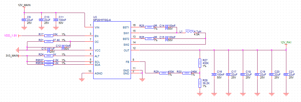
We used 2 MP28167GQ-A chips on our board. The board’s input voltage is 12V, output voltage is 12V, and operating current is 0.5A. The circuit diagram is as follows.

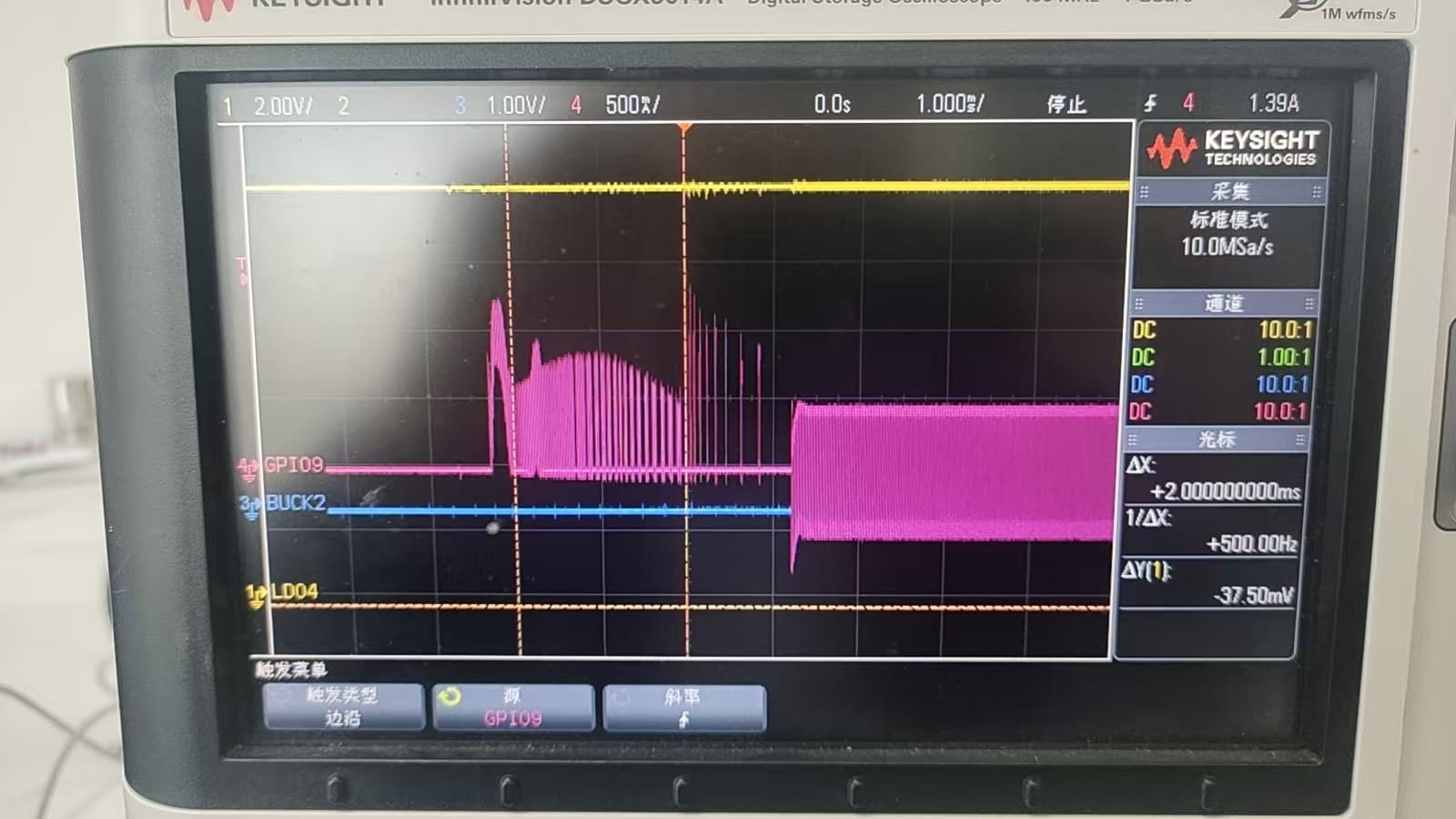
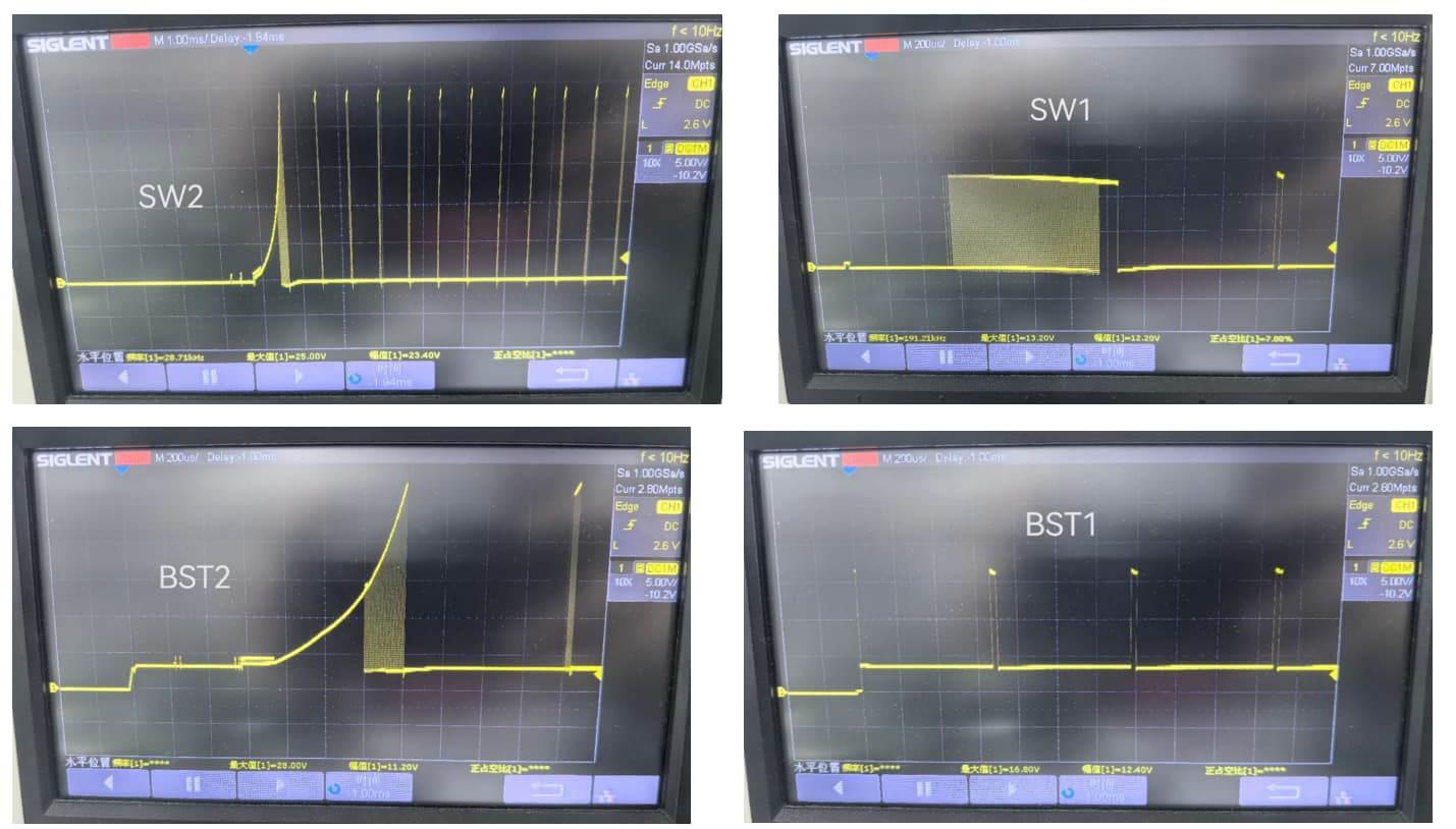
Currently, we have produced 5 batches totaling 5,000 boards, and on average, about 3 MP28167GQ-A chips fail per batch. The failure symptoms include: VIN to GND impedance of 0Ω, VCC to GND impedance of 0Ω, EN to GND impedance of 0Ω, and abnormal output voltage (22V、2.5V, 0.16V, etc.). We have sent 3 of these failed chips to your company for failure analysis, with FA numbers FA77858 and FA78101.

Please help us check if there are any potential issues with our design. Thank you.

Hi @kun.chen ,

Your design looks okay, nothing major that sticks out to me. As we wait for failure analysis, can you help answer the following questions:

  1. What is VDD_1.8V connected to? Is this from another IC, and if so, is that IC failing as well?
  2. Is the load constant, or does it change?
  3. Does failure occur at start-up, steady-state, shut-down, or load change?
  4. What is the working mode (FCCM or PSM)?
  5. Do you have any waveforms of VIN, OUT, SW1, and SW2?

Thanks,
Rubas

Hi Rubas,

Thank you for your reply

  1. VDD_1.8V is this from another IC,and that IC is not failing.

  2. The load current is not constant. At startup, the current of the inductor is at most 1.5A. In steady-state, the current is less than 0.5A.

  3. Because the chip only powers the RF unit, its failure only affects the RF unit and does not impact other units. Therefore, we are not sure at which stage the failure occurs.

  4. We did not configure the chip registers via I2C, so the working mode is determined by the default register values.

  5. The figure below shows the waveform with an input voltage of 12V and an output voltage of 22V.(VIN =12.28V, VOUT = 22.01V, EN = 1.79V, VCC = 3.66V, FB = 0.12V)