Hi Expert,
I’m using MP28167 with 5V Type-A adapter power supply for Vin. The output voltage is 5V~6V and the loading is very light so that it is working under PFM mode.
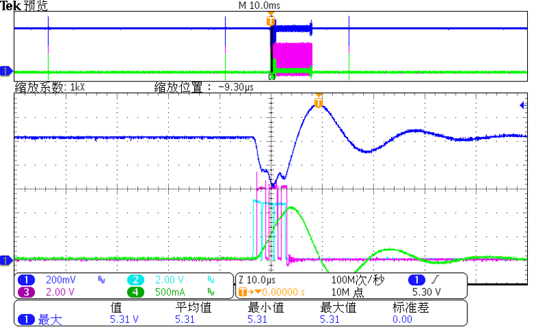
We found that the Vin Voltage would exceed the OVP limit at the time the pulses end as below figure.
I think add more input cap may solve the problem. However, the layout and components are not allowed to be changed here.
Is it possble that we can solve this issue by changing the registers?
Thanks in advance!
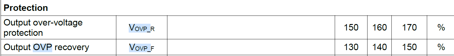
MP28167 is a standalone part with a fixed 5V output and it can handle the OVP as per the below snapshot from the datasheet. It does not have any I2C interfacing where you can vary the limit with the registers.
Hi Adhish,
Thanks for your reply.
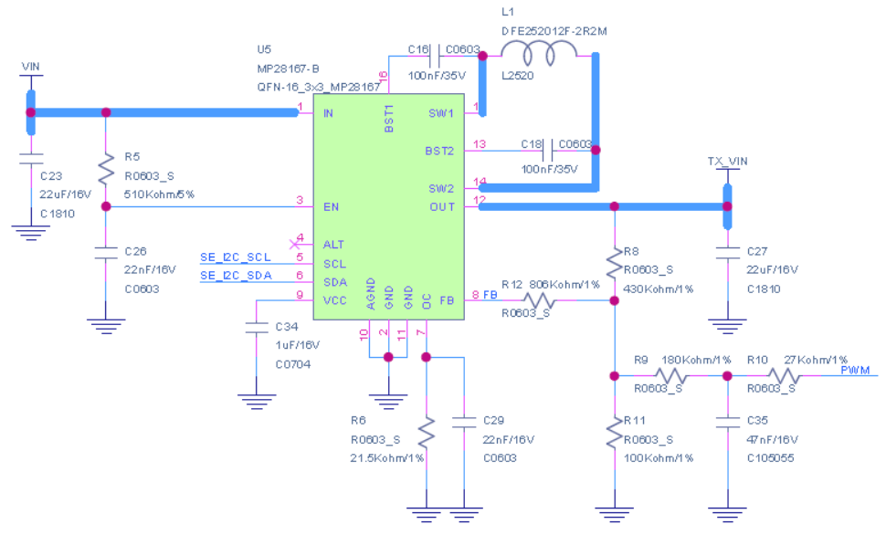
Sorry I’ve made a mistake of the PN. We’re using MP28167-B with I2C.
It’s not OVP of our converter triggered but the OVP of input Type-A interface.
The output votlage is 5V and the OVP limitation is 5.2V.
You can see the CH1(blue) as Vin of the waveform that the max value reaches 5.31V during PFM once the pulses come.
The channels are as below:
CH2(light blue):SW1 CH3(purple):SW2 CH4(green):Input current
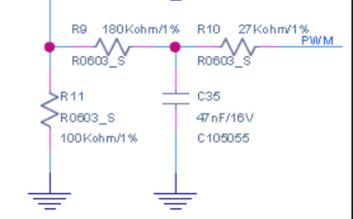
The schematic:
I wonder if there’s some internal methods such as on-time program or compensation adjustment with registers that we can config to reduce the quantity of pulses for each burst to reduce the input current and avoid this input voltage ringing.
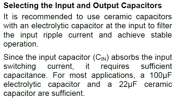
As per the datasheet, it is highly recommended to add atleast 2 of 22uF if not adding an electrolytic capacitor at the input side to reduce the shoot-up of the voltage.
I understand you cannot change the layout. However, you can just stack a couple of 22uF at input side cap one above the other and try checking that?
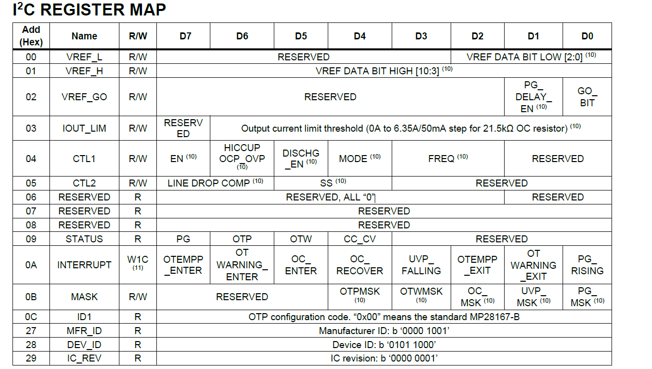
Because, unfortunately, in the resistor MAP as well, I believe there is no such setting that can control the on-time or do some adjustment for the input.