I think to choose MP28167-A buck-boost converter for my application, where I need VOUT = 12V, IOUT,max = 200mA with VIN,min = 4V and VIN,max = 14V.
But I am confused with inductor value calculation.
In the MP28167-A datasheet equation (2) estimates Lbuck inductor value in buck mode and equation (3) estimates Lboost inductor value in boost mode.
With those design parameters, considering fSW = 500kHz, 40% current ripple, 85% efficiency, I get Lbuck = 42uH and Lboost = 188uH.
Are my calculations right?
Should I consider the maximum between Lbuck and Lboost calculated values?
What is the VIN values considered for the L (uH) values reported in Table 1 for common output voltages?
With VIN = 4V the MP28167-A can still supply IOUT,max = 1A at VOUT = 12V, right?
I bought one EVL28167-A-Q-00A evaluation board and I changed the feedback resistors to have VOUT = 12V. With VIN = 4,2V and IOUT = 200mA I see high ripple on VOUT. Is the 4.7uH inductor value that causes the VOUT ripple?
Hi Alessandro,
Welcome to the MPS Forum!
Regarding your inductor calculations, according to my own calculations those values are correct. Though those values seem very large. I will note, for most applications 4.7uH would be sufficient for 500 kHz operation.
Is 200 mA the absolute max or nominal load current? I would typically advise to design for worst case scenario, say 1A peak load.
I would recommend using a 10 uH inductor before moving to the 42 uH. I would choose an inductor based on which operating mode you will be in a majority of the time. Is there a nominal operating voltage at the input?
To address your other questions:
The calculations use Vin = 12V with dIL = 40% of load current assuming max 3A.
Yes, the converter should still be able to operate with Vin = 4V, Vout = 12V @ 1A as its well within operating range.
There are a few factors that can cause a high ripple at Vout. The inductor is one key player in the output ripple. To reduce Vout ripple you can increase the output capacitance or increase the inductor size, try 10 uH.
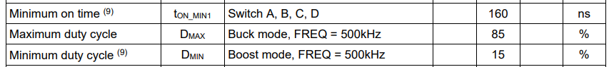
One thing I would like to point out, when operating with this buck-boost part, consider the following minimum on/off times and duty cycles for the converter given the wide range of Vin and Vout.
Thank you, Stephen.
In my application 200mA should be the absolute max load current with a nominal VIN = 12V.
I will try first to increase the output capacitance.
How should I consider the on/off times and duty cycle given my VIN range and VOUT = 12V ?
I added 330uF 35V electrolytic capacitor as C2 on my EVL28167-A-Q-00A evaluation board; the 4.7uH inductor is still present.
With IOUT = 200mA, when VIN decreases under 4.3V, now I see much less ripple on VOUT then before, but VOUT decrease from 12V to 7V about. Then VIN must increase over 6.3V to have VOUT = 12V again.
If I start with VIN = 4V, VOUT = 5.9V with a little ripple. Again, I have to increase VIN over 6.5V to have VOUT = 12V.
I think L = 10uH is needed at least, right?
What about your MPL-AL6060-150 inductor? Could L = 15uH be suitable to have VOUT = 12V @ IOUT = 200mA with VIN = 4V?
For example, operating at Vin = 4V, Vout = 12V, Iout = 200 mA the duty cycle for a boost is given by 1-(Vo/Vin). So duty cycle will be about 75%. This is more relevant when working with voltages near the output voltage.
Larger values of inductor current ripple allow the use of lower inductance, but results in
higher output voltage ripple and greater core and power device conduction losses. A smaller inductor value will store energy faster and result in a higher inductor ripple. Since the output current is so low, the FET’s will be switching for a shorter amount of time, which can result in a lower output voltage.
Increasing the inductor will slow the rate at which energy stored, which can reduce the current ripple. Try 10 uH first and check the response, if more reduction is needed you can try the 15uH. The MPL-AL6060-150 may be suitable for this.
Hi Stephen, I come back to my application with MP28167-A buck-boost converter. Now I have two my board, one with L = MPL-AL6060-100 and the other with L = MPL-AL6060-150; both have COUT = 22uF (tantalium) x 5 + 330uF (electrolytic).
I need to boost VOUT to 12V when VIN = 4V and load is less then 200mA.
With no load I get Vout = 12V with VIN = 4V on both my boards.
But with 50mA load I get the best VOUT = 9V only with L = 15uH.
Nevertheless, MP28167-A should feed up to 1A with VIN = 4V and VOUT = 12V (rif. datasheet, page 10, “Recommended VIN, VOUT, IOUT Operation Range” graph).
How can I achieve that?
Should I use L = 22uH ?
Using I2C interface was not planned on my board, but the I2C interface is available for an external master unit through a header connector.
May some (not-volatile) settings through I2C interface help to get my goal (VOUT = 12V, IOUT,max = 200mA with VIN = 4 ÷ 14V) ?
May your MP28167-B or MP28167-N different parts be a best choice for my application?
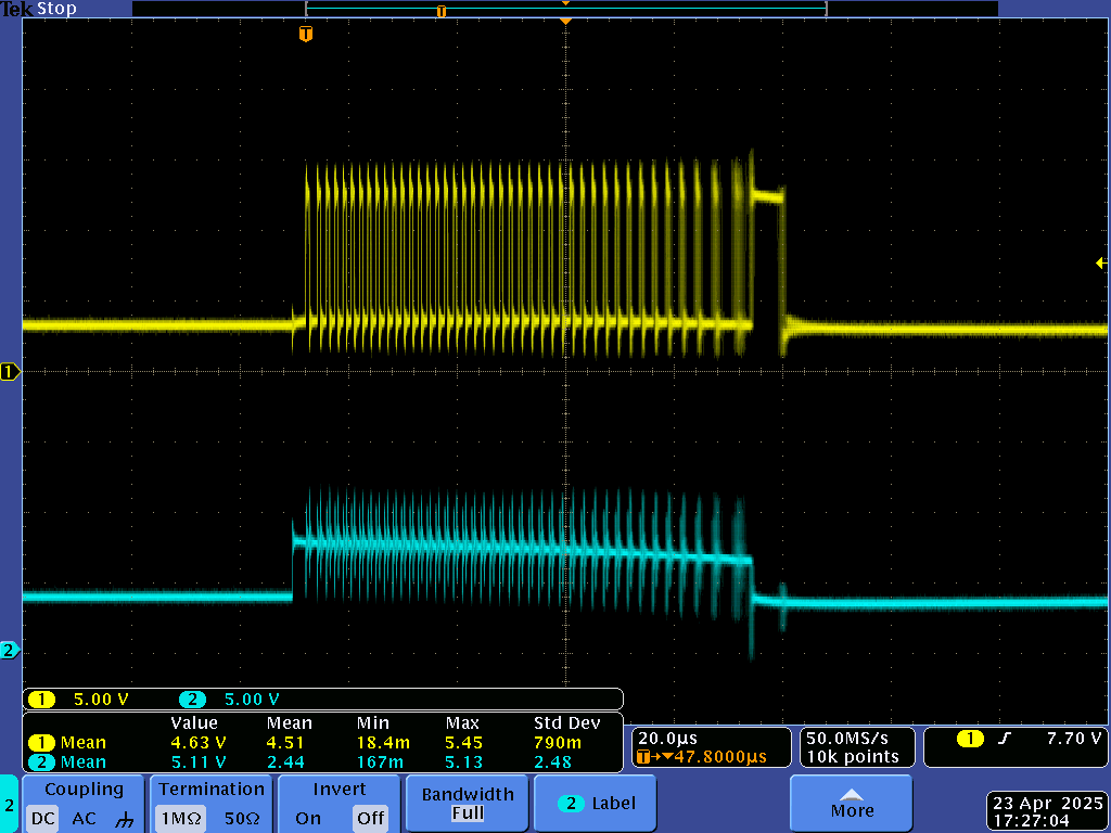
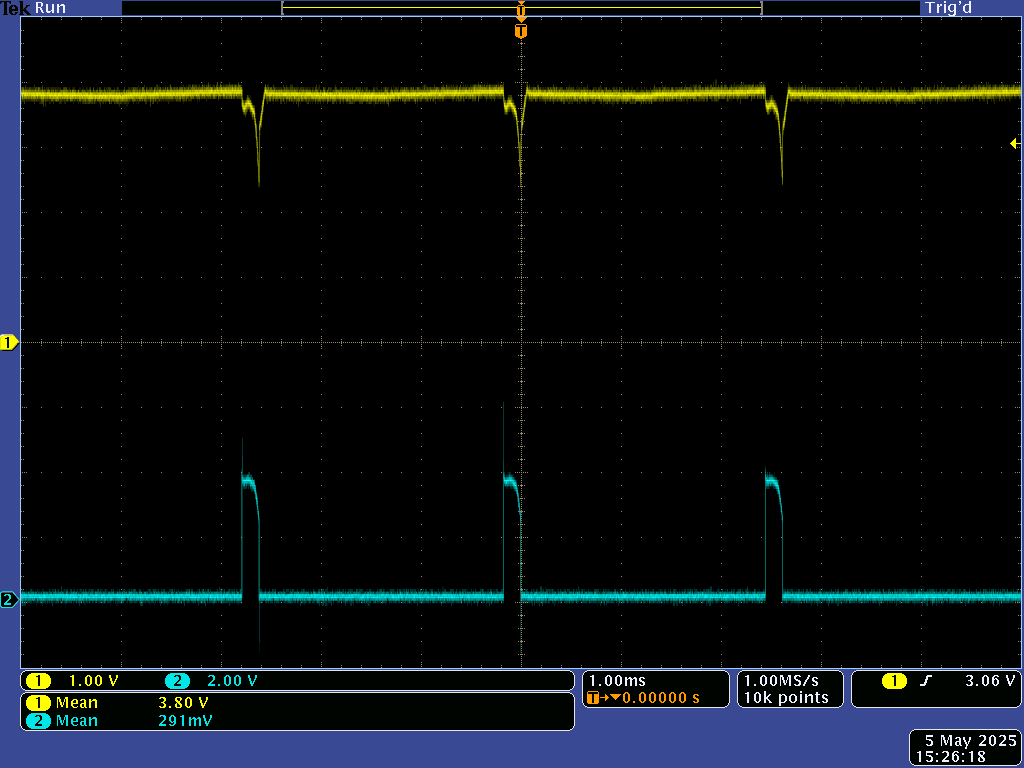
Attached is the scope screenshot of the waveforms on pin BST2 (yellow) and BST1 (cyan) of MP28167-A when VIN = 4V and IOUT = 50mA.
Both the waveforms have 2.5ms period.
Can you explain me what MP28167-A is doing in that condition?
Hi Alessandro,
Apologies for the delay. Is the lower output voltage only occurring on one of your boards or both?
How does the IC work at higher loads? For a 200-mA load I would suggest changing to 22uH.
I would like to check your schematic. Can you please provide a snippet of the schematic with component values?
I do not believe any I2C register values would affect overall performance. I would like to check the values regardless. Please use the MPS Virtual Pro Bench GUI to read RAM, export as a .txt file and upload to this thread.
Additionally, to ensure we know what is happening, please probe the SW1 & 2 node, PG, and FB. Waveforms for SW, VIN, and OUT would be helpful.
Finally, just to check all of our boxes, ensure your power supply is not being limited by the output current. When operating in boost mode, the input current will be higher.
Hi Stephen, now my board is not available to make measures, but I think you can get the same boost behaviour with your EVL28167-A-Q-00A evaluation board.
I connect VIN to my 4V@2A DC power supply and VOUT to RL = 157 Ohm (to simulate IOUT < 80mA @ VOUT = 12V). On my EVL28167-A-Q-00A I already changed the feedback resistors with R1 = 430K, R2 = 39.2K and RT = 787K to have VOUT = 12V. Inductor L1 is the original 4.7uH. I already added 330uF 35V electrolytic capacitor as C2. In this configuration I get VOUT not more than 10V and the board consumption is about 200mA.
Attached are the following scope screenshot:
VIN vs VOUT
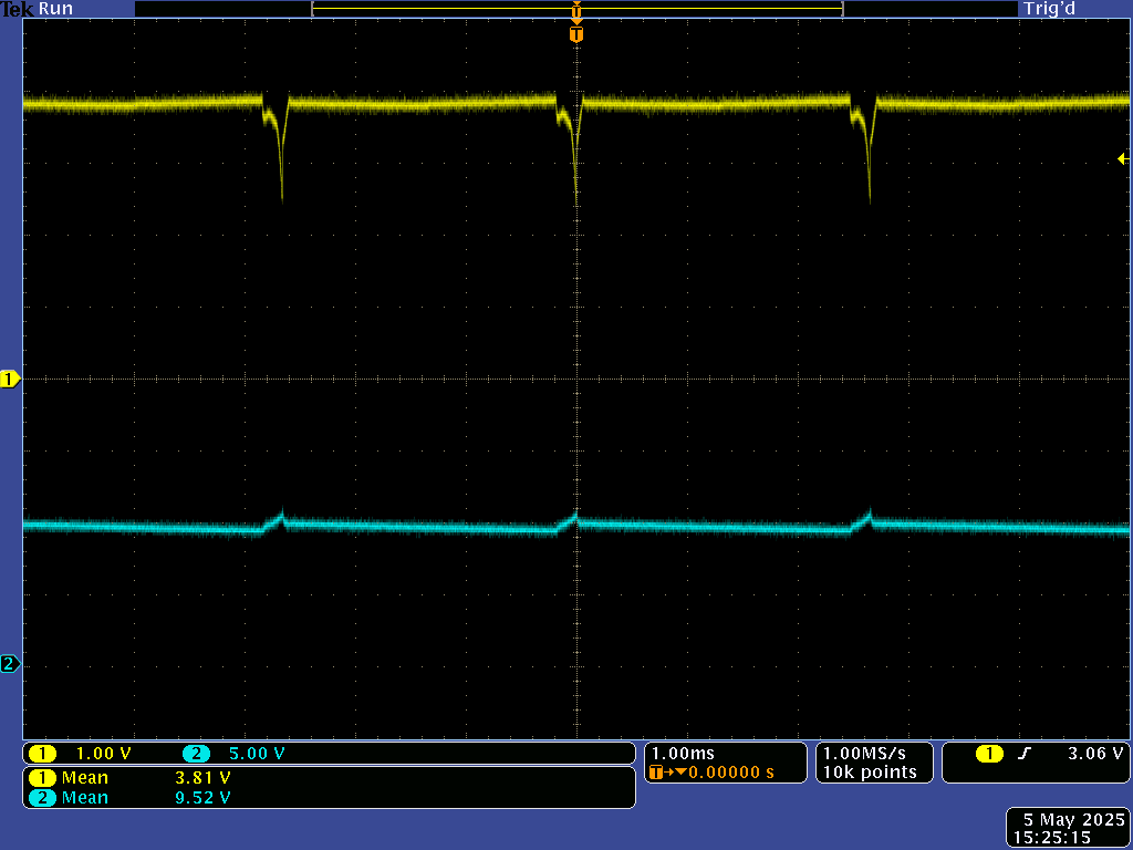
VIN vs SW1
VIN vs SW2
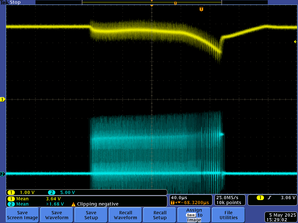
If I add 4700uF/25V electrolytic capacitor on VIN, then the VIN drops appear only for a short time at the board power-on, than VOUT becomes 12V steady.
My board schematic with MP28167GQ-A is the following:
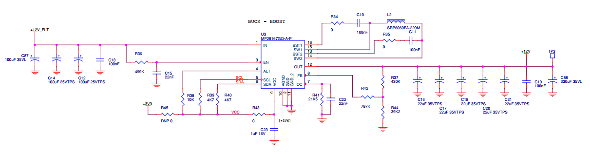
Now C14 = C12 = 100uF/25V (tantalium chip), C87 = 100uF/35V electrolytic, L2 = 22uH (SRP6060FA-220M) and we keep C16 = C17 = C18 = C20 = C21 = 22uF/35V (tantalium chip) and C88 = 330uF/35V electrolytic.
This configuration seems to properly boost VOUT = +12V without considerable ripple at IOUT = 50mA when VIN = 4V.
I would like to know if this configuration can be considered stable for our application or the issue may happen again due to components value tolerance or room temperature.
I would like to know how is possible to get VOUT = +12V and IOUT = 1A when VIN = 4V, as reported in the datasheet.
Hi Alessandro,
I have checked the component values you have shared with via simulation and lab testing. I can confirm the component values will work for 1A output @ 12V. If this implementation does not work, I would suggest you look at the layout for your implementation.
Taking a look at the inductor, it has fairly high DCR which can limit performance. I would suggest finding an inductor with a lower DC resistance, but 22uH is OK.
This topic was automatically closed after 18 hours. New replies are no longer allowed.
Hi Stephen, now I have in-rush issues on my board.
Actually, there is a lot of capacitors to charge at start-up…
In one of my product configuration the power supply for my board is +5V and 1A current limited: this power supply continuously trips (hiccup mode) in overcurrent protection (OCP) when power on my board. With a lab power supply with a much higher current limit threshold I see many current absorption peaks in the first 50ms from the power-on: the first one is about 2,9A, the others about 1A.
Any idea on how to reduce the in-rush current? Is it possible to have a strong soft-start?