the MP2770 will require an external PD controller to negotiate the power levels
Yes I’m aware of this. Thanks for pointing this out! This is a critically design relevant point.
pass-through mode per the datasheet seems to limit the input voltage to 5V
I think this is a misinterpretation. This datasheet section is meant to be an example of the pass-through over voltage protection behavior.
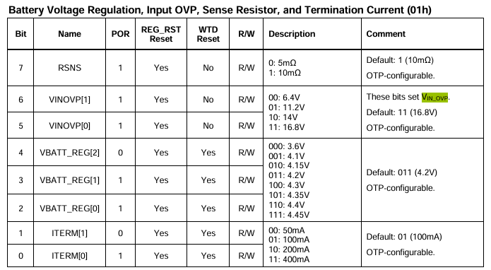
Because VIN_OVP is configurable and will be set by the host, depending on the requirement of the SYS load. The default of VIN_OVP is 16.8 V to enable a max VIN of 16 V (which is VIN_MAX per specs).
As you can see, VIN_OVP is configurable.
This means, if my application anticipates a VIN of 16 V, i set the VIN_OVP to 16.8 V. If 16 V will be overvoltage in my application, because it only anticipates e.g. 9 V as max VIN, I would lower the over-voltage protection accordingly for proper fail-safe management (error reporting and behavior of the MP227) as in this scenario a VIN of 16 V could indicate a serious damage of the whole system (depending on how VIN is generated).
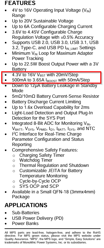
I believe the device is definitely designed to deliver these outputs of 16 V/3.65 A.
This is what I have found about boosting input too VSYS (VBST):
These specs (16 V at 3.65 A) couldn’t be achieved if the voltage VIN had been limited to 5 V. This output has to be stable independent of charge modes in order to keep the system load stable.
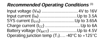
So I don’t think it is possible to supply that much power into the IC since the max input current is 3.5A.
Could you please verify that the device meets my requirements or recommend an alternative device that can meet them?
Because the Datasheet states that the max input voltage is 16 V, which I thought will allow me to negotiate a PD contract of 16V/3.5 A (USB PD 1.3) or 15 V/3 A (USB PD 3.0), given the max input current of 3.5 A.
This yields a 45 W power budget if a PD contract of 15 V/3 A is negotiated (by an external PD controller) of which I assumed the MP2770 is able to convert to the following internal rails (based on the limits I’ve found in the datasheet specs) using its internal buck converters.
a) charging rail: 4.2 V at <=6 A ===> ~25 W
b) SYS rail: 4.3 V/3.65 A ===> ~16 W
Total: ~41 W
If you were misinterpreting the configurable over-voltage protection feature, then the MP2770 should be able to output 4.3 V/3.65 A (or theoretically 16V/3.65 A) to SYS.
Do you agree?