Hello,
I’m working a project, where I would like to use the MP2672 to charge two 18650 cells in series. My problem is that MP2672 gets hot quickly (in 2-3 seconds to above 100°C) even though I’ve set the charge current to 500mA.
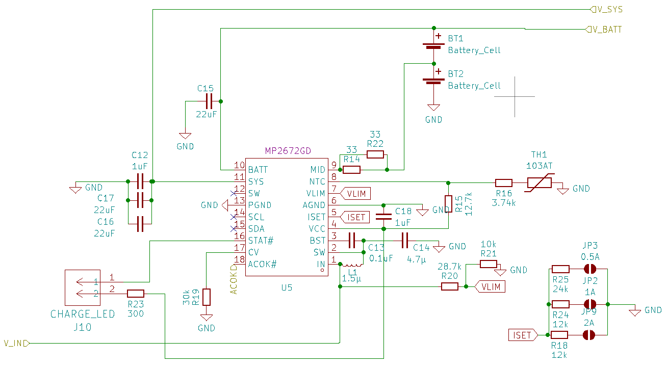
Here is the schema:
I’m aware that C14 is at the wrong place, it should be between IN and GND. This is due to an error in the original schema which I had to work around but I would not expect this to be the cause?
V_IN is attached to a 5V USB-C Notebook charger. It should be able to provide enough current. V_BATT and V_SYS are connected to a disabled circuit.
The solder bridge JP3 is closed connecting the 24k resistor to ISET which should give a charge current of 500mA. ACOK and STAT are connected to two LEDs. Both of them are solid on as soon as V_IN is connected.
This is the inductor I’m using: https://jlcpcb.com/partdetail/Sunlord-MWSA0603S1R5MT/C408444
If the batteries are not in place, MP2672 gets to about 30°C. As soon as the batteries are connected, it heats up quickly to above 100°C. The heating also happens If I add a load (< 500mA) to V_SYS without batteries installed.
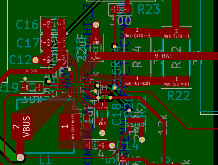
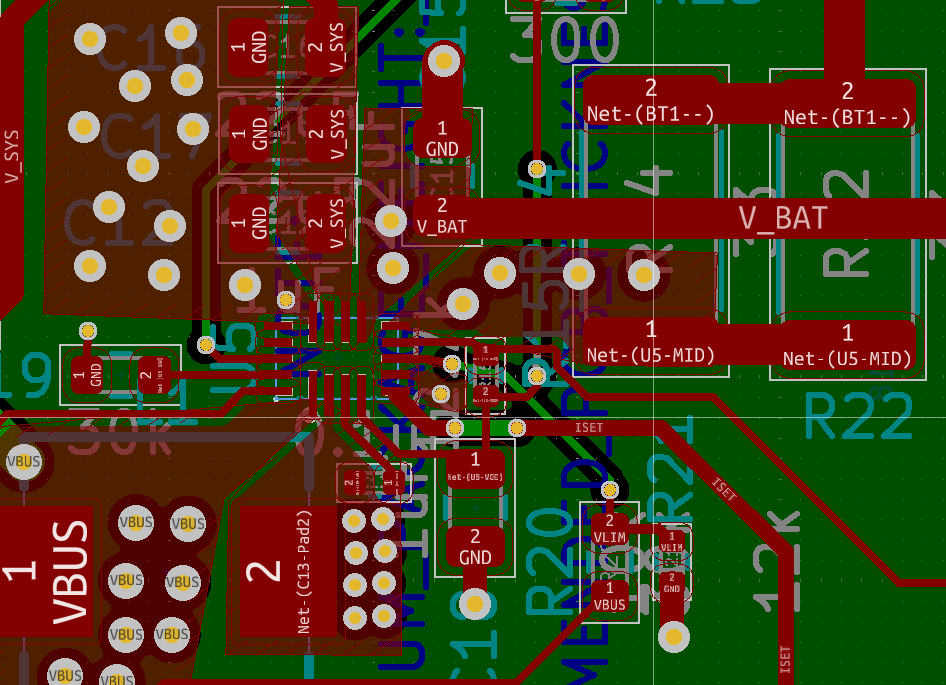
I’ve already compared my schema with the reference design but could not find the error. The same issue happens on two different PCBs.
Since I’m a hobbyist engineer, I’m a bit lost on how to further debug this. Would be great, If someone could guide me to the right direction.


