Dear Team,
regarding this battery charge I kindly ask you what should be the time needed to switch from VIN to BAT when the main power at VIN is removed and similary what shoud be the switching time needed to change the path from BAT to VIN when the main power at VIN is restored.
In other words on the SYS output pin, when the system lost the main VIN and the system activate the boost function or when the system is in boost mode and the VIN main power is restored there are some glitch or temporary power loss on the output SYS voltage due to the dynamical changing of the internal power path?
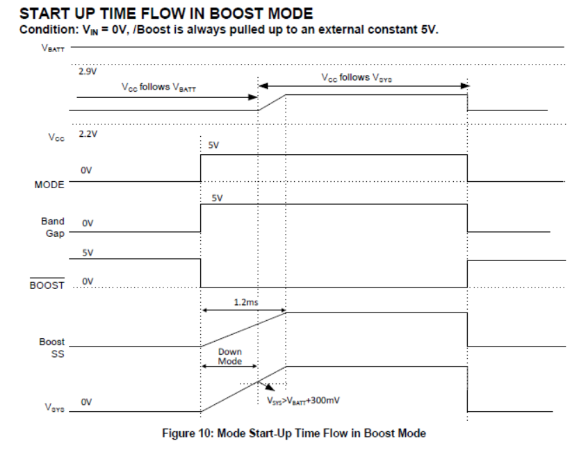
It looks like Vsys comes up to set voltage about 1.2ms after MODE goes high in this graph. This is likely a typical value, but expect the delay when switching MODE to be around 1.2ms on the output. You may want to try testing this out yourself on an evaluation board to make sure the performance acts as expected when switching between charge and discharge functions.
Thanks,
Brendan Schoemehl
Field Applications Engineer
Monolithic Power Systems | MPS Now
Thank you Brendan,
my think was to use this charger, together a small microcontroller, in order to get it acting like a small UPS unit. In that sense when the main power supply is attached to the VIN input, the MP2637 simply has to power the load attached to the SYS pin and also if needed perform the battery charging task, but when the VIN power supply is removed or in the event of a sudden blackout the MP2637 should be able to switch automatically to the battery mode (in this sense the microcontroller should be drive properly the MODE pin).
In this application is fundamental that the time related this power path change is “very small” in order to avoid any power loss experiency regarding the load that is powered from the SYS output pin. In a similar way, when the main VIN power is restored, the power path change have to act in a same way so with a “very small” time to avoid again any power loss to the load.
The main advantage that I can see in using such type of integrated battery charger is that the needed external components number is very small due to I’ve only a one inductor used as a buck stage in charging and as boost stage as supply, but my doubt is that with this topology may arise trouble into the dynamical behavior related to the power path changing.
Also using a microcontroller to check about the input voltage (e.g. by means of an external voltage supervisor with fixed threashold attached to an interrupt input) and then subsequently by driving the MODE pin properly (working under interrupt this is a matter of some micro-seconds) if the boost stage take 1.5 ms to switch on I can have a potential cut of the output power (due to a voltage output decreasing) with a entity strictly related to the output current drawn from the load and the overall switching time needed to reconfigure the power path.
Suppose to have a load that require a maximum output current of 1.5 A at 5V nominal and that this load require a minimum working voltage greater or equal to 4.8V, with a switching time of 1.5 ms we have to use an output capacitor equal to, at least, 11.25mF that is clearly unapplicable for many reason, hence the only other parameters on where we can work is the power path commutation time, but this is fixed because related to the used topology, hence I think that is not really possible to achieve this particular behavior with this type of system.
Could you please let me know your thinking about these point?
Thanks and best regards.
F.
You are bringing up lots of or concerns that I believe need to be looked into specifically for your application and set up. My suggestion is to order an evaluation board and test the device out to see how the power path delay affects your system in a practical field test. By testing the device out within your system, you will have an accurate idea of how everything will perform together in the real world. The You can order a MP2637 evaluation board directly from here.
Keep in mind, the graphs from the datasheet only show start up times and recoveries, they are not showing when the part moves from charge mode to boost mode and vice versa. There may not be a delay switching modes when Vsys is already high. Note in the above graph, Vsys was originally low, hence the delay in bringing the system voltage all the way up to spec. This will be something you want to check in testing because there may be minimal delay in switching from input to battery (and vice versa) with you toggling the MODE pin with a micro when Vsys is already high.
Thank you Brendan,
when you wrote " There may not be a delay switching modes when Vsys is already high" if VSYS is high this means that the system can work in two modes, charger with applied VIN or battery sourcing.
Let me try a reasoning, suppose the VIN is applied so the system is working in charging mode, hence Q1, Q2 are closed instead Q3 and Q4 are working as synchronous Buck DC-DC topology, now if the power supply is removed the system have to block Q1, Q3 should be act as a diode from SW to SYS and Q4 work as a switch to emulate a Boost DC-DC topology. To avoid any short between the SW side and the VIN side there must be a dead time, this should be investigated because has to be very small in order to avoid the need for big capacitor on the SYS output and then a possible temporary blackout on the SYS pin. Similary if VIN is put again the logic have to be reversed hence before Q1,Q2 get the VIN to SYS the Q3 and Q4 have to change the behavior, then some time is needed again to perform this operation and again a possible temporary blackout can be originated. Now the question is how long this time should be…
In order to perform some checking without the hardware is possible to use the MPSmart v8 in order to do some simulation?
I’ve also checked the MP2696A chip, this seems quite similar, from this forum (MP2696A switch over time) I can read that:
“After setting the BST_EN bit high and Vin drops below 2V, the device takes 3ms to switch from buck mode to boost mode.”
this can be a useful info, also I kindly ask you about the DM-DP output port if is possible avoid to use them and get the output directly on a power mosfet used as a switch to power on and off a load in a controlled manner. In other words the output can be opened or closed when the load have to be disconnected or connected upon some conditions.
There should be an interruption in current to the system when going from charge to discharge modes but I’m not sure what to expect on the output of the system Vsys without testing it out. I would love to simulate it for you but the device is not available in MPSmart based on our database. While it would make the most sense for the device to interrupt the system voltage when changing modes for the reasons you listed, I did not want to confirm this would happen without having the evidence from the datasheet or testing. The MP2696A is a similar device and given that my colleague has found that the device needs 3ms to go from charge to discharge, I am going to say that we can expect similar delays to the MP2637.
Yes, you can avoid using the DM and DP pins, these are just used for USB applications. If you are not using USB, disabling these pins is an option.