I used the reference design and values mentioned in the datasheet and created by own PCB.
I sent the files to JLCPCB and let them assemble it for me.
Schematic:
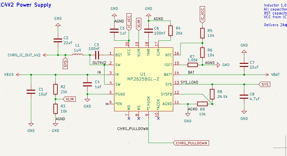
my intended values are:
VLIM = 4.75V (defined by the VLIM voltage divider)
ICHRG = 2A
SYS = 4.2V (defined by the SYSFB voltage divider)
The boards arrived 2 days ago.
Fresh out of the box i started testing if everything works as intended.
The behaviour of the MP2625B on my board are as follows:
When Input Voltage is 5V and no battery is connected:
![]() SYS is at 4.2V (as defined by the SYSFB voltage divider)
SYS is at 4.2V (as defined by the SYSFB voltage divider)
![]() CHRG-LED is blinking fast indicating no battery is present.
CHRG-LED is blinking fast indicating no battery is present.
![]() VCC_Pin is ~4.5V
VCC_Pin is ~4.5V
Everything works as intended.
When Input Voltage is 5V and the battery is connected:
![]() Input Voltage drops to VLIM at ~4.75V (as defined by the VLIM voltage divider)
Input Voltage drops to VLIM at ~4.75V (as defined by the VLIM voltage divider)
![]() VCC_Pin is ~4.5V
VCC_Pin is ~4.5V
![]() SYS drops slightly to 4.16V
SYS drops slightly to 4.16V
![]() CHRG-LED is on and battery is charging in constant current mode.
CHRG-LED is on and battery is charging in constant current mode.
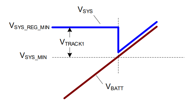
When no input voltage is present so everything is powered by the battery:
![]() SYS equals VBAT (it should be 4.2V!)
SYS equals VBAT (it should be 4.2V!)
![]() VCC_Pin is 0V (it should be ~4.5V!)
VCC_Pin is 0V (it should be ~4.5V!)
When the chip runs on battery power i assume the charge pump is disabled.
It is like the EN pin is high and the chip is turned off so VBAT gets passed through to SYS.
In my design i left EN floating, because i dont need it and i assumed the pin is pulled down internally already. But in my tests i also connected it to ground just to be sure, but still the charge pump is not turning on on battery power.
Also if the EN pin is the culprit then charging wouldn’t work. but it is.
Because i studied the whole datasheet and overthinked every design choice i made, I am either blind or the IC is indeed broken?! But it’s also my first time designing PCBs, so someone enlighten me please ![]()
Kind Regards
Max