Hi, Expert,
When we use MP2491C to output 0.5V, What are the maximum input voltage and minimum output voltage to ensure normal operation? The range provided in the datasheet is 4V~32V, what is the actual value?
Hello,
The device covers a wide range of input and output voltages. The range being 4V-32V input and 0.5V to 30V output, therefore can be designed to meet all potentials for stepdown. You can refer to the application circuits in the datasheet as well for reference circuit.
In your design, you want to implement Vout of 0.5V, I recommend using a lower input voltage like 5V.
Regards,
Nouman
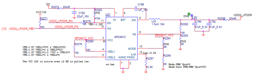
We designed the application scenario as the following shows: Vin:8~12V, Vout=0.5V, for LPDDR VDDQ power. Is there any risk in using it like this? And why did you recommend 5V Vin, could you tell me the reason?
Hi Ian,
Initially, the specs were not mentioned. The reasoning behind it is that this device uses COT control to regulate the output.
I used 5V to 0.5V conversion as an example since its still sufficient and reliable with the 10% duty cycle. It also meets the minimum on time requirement.
You can confirm your design too, by calculating the on time period and comparing it with the sw frequency. ( T = 1/Fsw ) I think 0.5/12 duty cycle on time is quite low and close to the minimum on time Ton_min of 60ns.
From the electric charachteristics chart:

Regards,
Nouman
Well, We used 12V Vin’s worst case is 12V(+10%)=13.2V. According to the calculation, 75.7ns is enough. If the min on-time=60ns can be guaranteed, can we think that there will be no problem with our design?
Hi Ian,
The component placements seem correct. Couple notes I would make:
- The PG pin must be 3.3V, I do not think it can work with a 1.8V potential.
- VSEL1 and VSEL2 pulled to VCC gives the 0.5V vref, and 5V Vout.
- Confirm the feedback network values.
Regards,
Nouman
Hi, Baryal,
Why did you say “it can work with a 1.8V potential”? Is there any risk that 1.8V is only used as the pull-up voltage of PG OD output?
Hi Ian -
PG pin is an open drain output, typically ran with logic threshold voltage or 3.3V. Also, helps with ensuring the output regulated voltage is reached.
Can you please confirm what your Vref is?
Regards,
Nouman
Hi, Baryal,
Vref we used is 0.5V. According to the Functional Block Diagram, it seems that PG does not affect output. How to explain it?
BTW, 1.8V pull-up voltage is not allowed? Can it work normally in the 1.8V pull-up?
Hi Ian,
On the block diagram, you may observe that the feedback is connected via couple PG comparators to the FET for PG pin. Please refer to Power Good section in page 16 of datasheet to understand the relation of output to PG pin.
Like mentioned before, it is not recommended to have PG pin at 1.8V. It must be 3.3V or 5V.
Regards,
Nouman