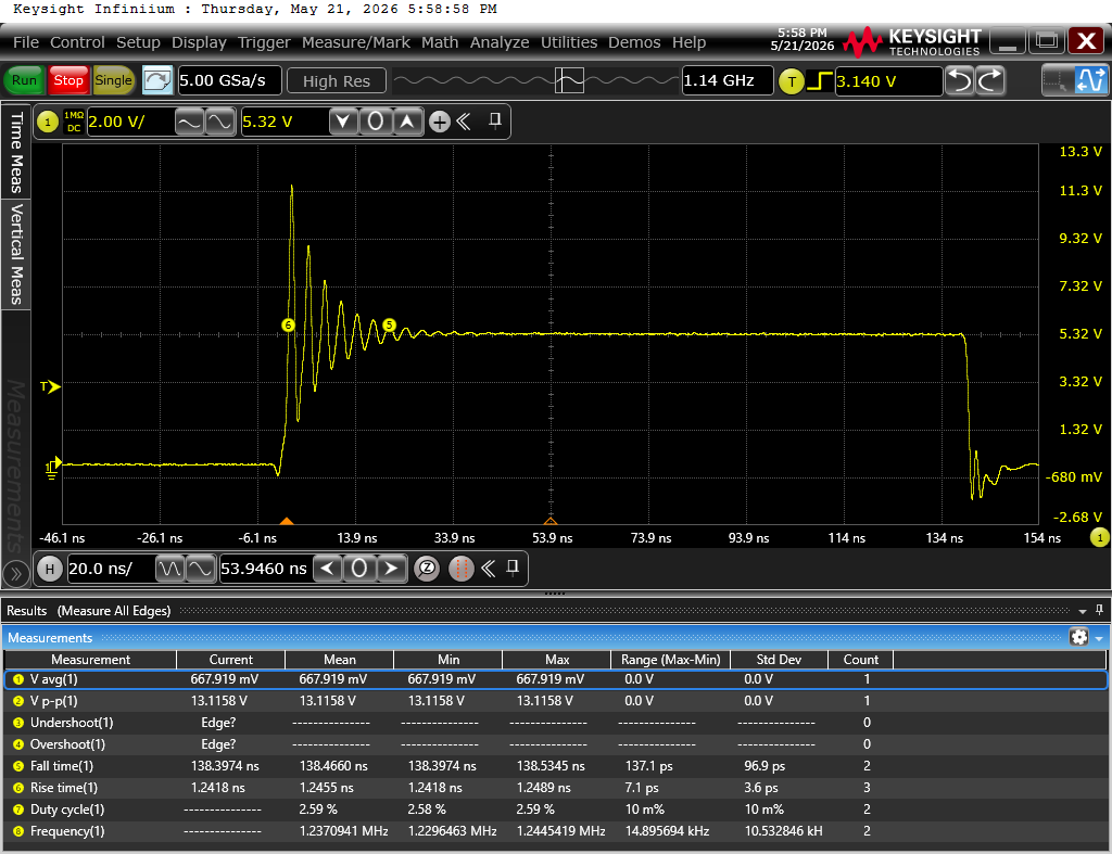
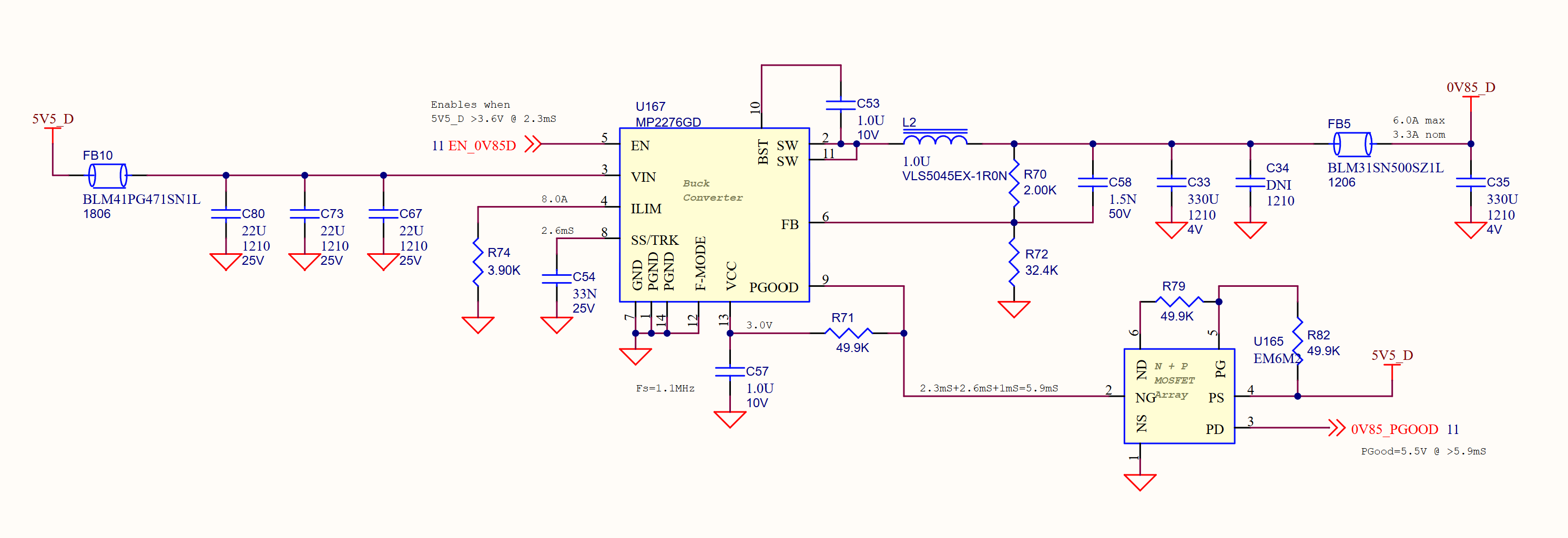
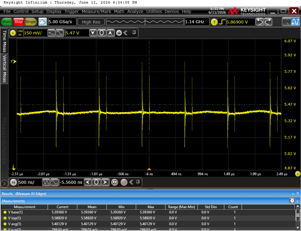
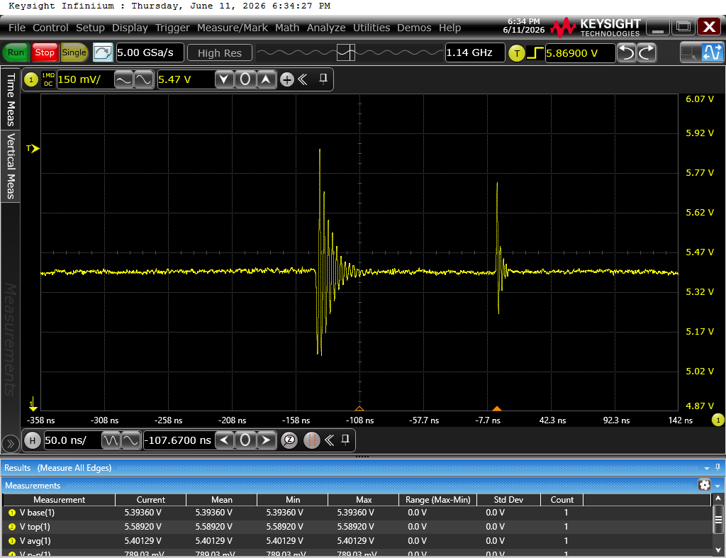
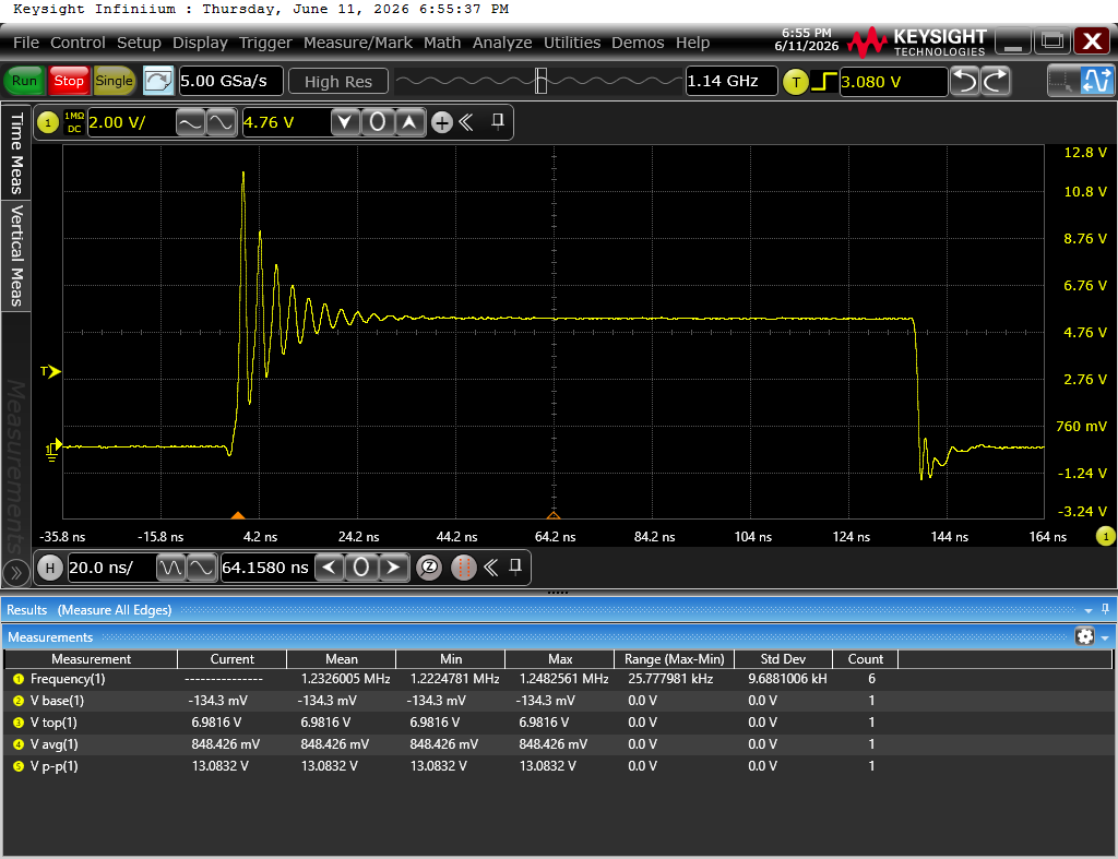
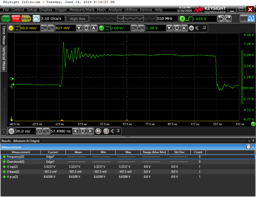
We are using MP2276GD bucks to generate 0.85 V and 1.2 V rails from ~12 V at 1 MHz. The rails regulate fine, but the SW nodes show noticeable ringing.
What is the recommended approach for reducing SW-node ringing on the MP2276GD?
Things we are considering:
Adding a small series resistor in the BST path
Adding an RC snubber from SW to PGND
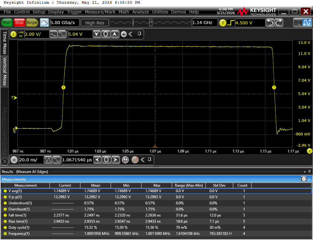
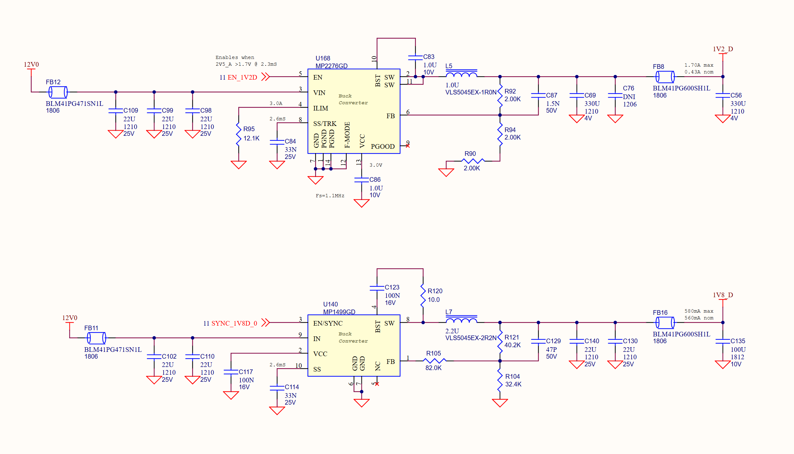
One reason we are asking about the BST resistor is that our MP1499GD rails on the same board have cleaner SW-node waveforms, and the MP1499GD reference circuits show a resistor in series with the BST capacitor. The MP2276GD reference circuits appear to only show the BST capacitor.
Is a BST resistor allowed/recommended on MP2276GD, or should we avoid that and use a SW-to-PGND snubber instead?
Thankful for any recommendation and guidance!
Attached snippets of our 0.85V SW node as well as one of our MP1499GD SW nodes (1.8V). I also attached a snippet of the schematics showing the 1.2V and 1.8V Switchers.
When probing the switch node, use spring tip ground with passive probe or a short lead differential probe to limit radiated noise coupling into the measurement. Place the probe tips as close to the SW / PGND pins as possible.
I notice the waveform labeled ‘085V SW Node’ is switching between approx. zero and 5V. That is unexpected. I expect it to switch between zero and 12V if Vin=12V. What is Vin supplied for this converter, and what load is connected?
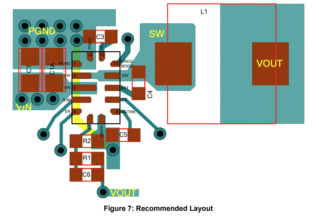
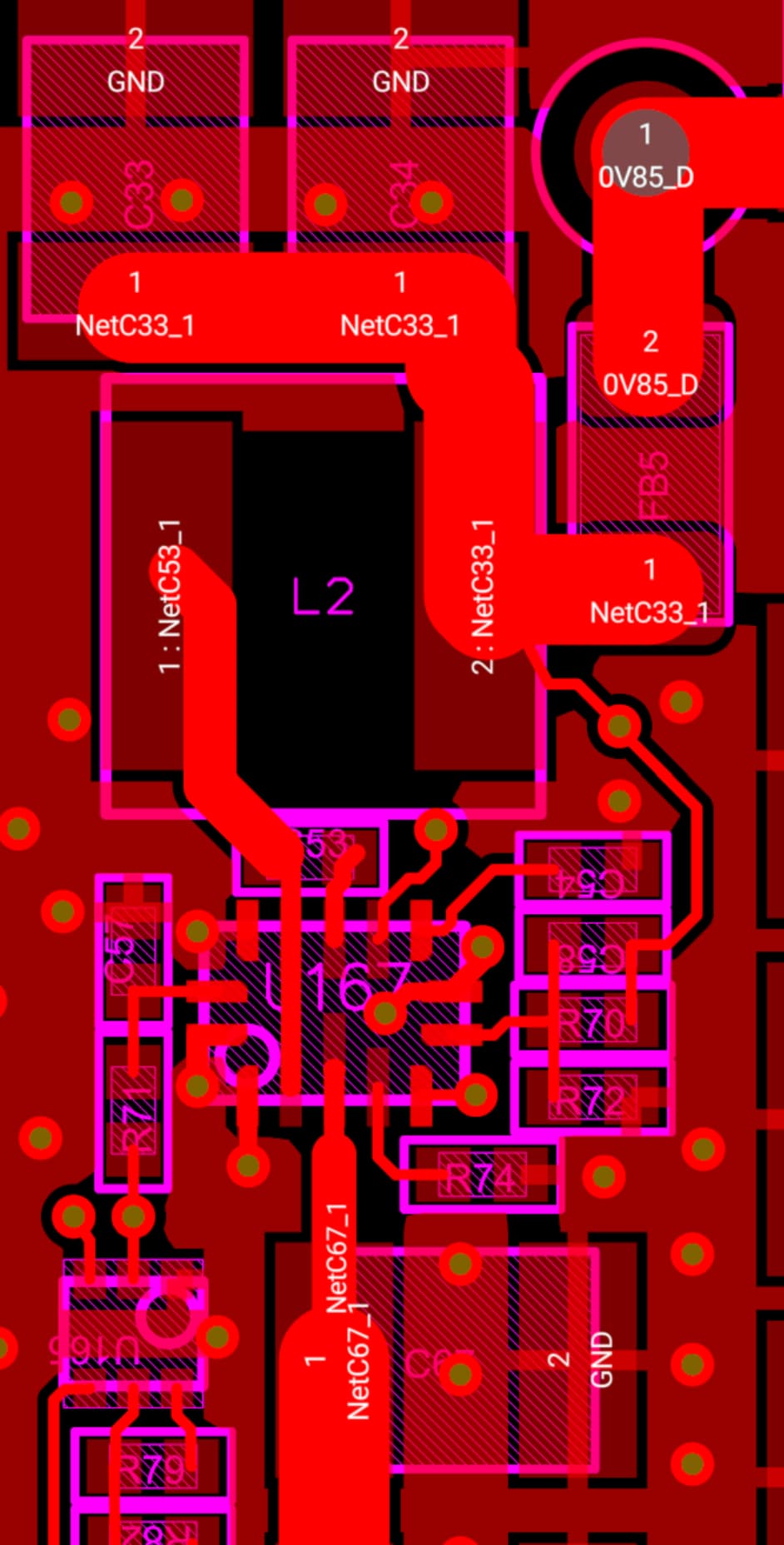
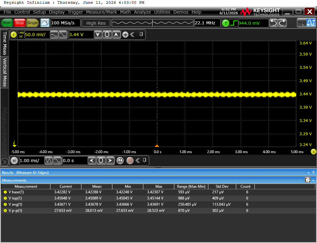
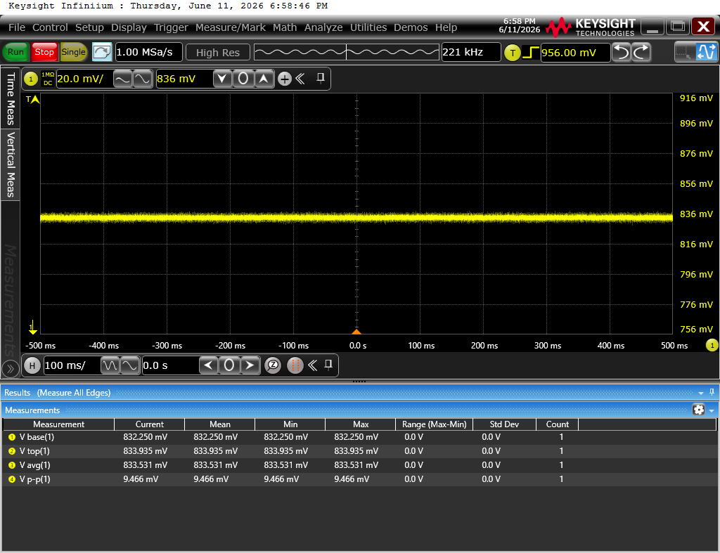
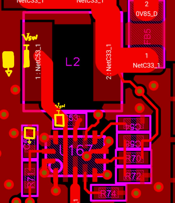
Please share layout of the MP2276 converters as well as Vin, EN, and Vout waveforms along with the VSW waveform.
Are you using the spring tip probe to measure VSW between the top of C53 and the ground of C57? You could also use the large ground plane next to the inductor if it is acceptable to scratch away solder mask:
Yes, using spring tip probe or lately an active differential probe in single ended mode across the SW Cap.
Yes, the dot on the inductor is on the SW node.
Furthermore, I ordered the devkit of the MP2276 (LINK) and swapped the FB resistors so that it creates 0.85V. I fed it 5.5V while using a DC load at ~4A and saw a waveform across the SW Cap that has some ringing but much less compared to my design.