I am designing a power amplifier board using the MP1918 Gate Driver with GaN FETs for a DC motor phase-switching application. I have a few questions regarding the grounding and power supply configuration:
AGND vs. PGND Separation: What is the technical reason for having separate Analog Ground (AGND) and Power Ground (PGND) pins on this device?
Shorting the Grounds: In the datasheet’s typical application circuit, AGND and PGND are shorted together (often via a 0Ω resistor or a net tie). If they are eventually connected, why are they defined as separate grounds in the first place, and what is the best practice for connecting them in GaN environment?Single vs. Dual Supplies: Do VCC1 (referenced to AGND) and VCC2 (referenced to PGND) require independent power sources, or can they share the same rail with proper decoupling?
Single vs. Dual Supplies: Do VCC1 (referenced to AGND) and VCC2 (referenced to PGND) require independent power sources, or can they share the same rail with proper decoupling?
I would appreciate your guidance on ensuring high noise immunity for this high-speed switching design.
Having a separate AGND (used for signal lines) and PGND (used on the FET side) is useful for noise-sensitive applications. Switching a FET is noisy, and directly sharing the ground between the signal lines and power lines could result in severe ground bouncing that can damage the sensitive GaN FET.
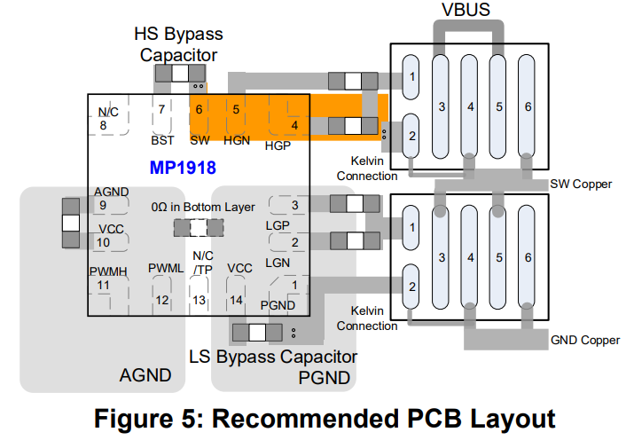
Connecting the two GNDs is to keep the reference the same, but the key here is connecting the GND planes. If you were to have a general GND plane for both signal and power, then the two can interwind noise easily. If you have two separate GND planes but connect them at a strategic point with a resistor or net tie to keep the reference the same, then the noise from the power GND will not bleed into the signal GND as easily.
Below is a layout example of how separating yet connecting the two GND planes would look. Notice how the signal and power GND traces are on the top side (dark gray), but the large GND planes are on the back side (light gray), which are separated and connected at a single point with a resistor:
Subject: Clarification on Ground Separation (AGND vs. PGND) for the MP1918 Gate Driver
"Thank you for the quick response. I have an additional question regarding the separation of AGND and PGND.
In the power boards I currently work with (mostly MOSFET-based), we incorporate an Isolator component to separate the input grounds. For example, the PWM input lines coming from the FPGA are referenced to Digital Ground (DGND), while the outputs of this Isolator provide PWM signals referenced to Power Ground (PGND). These PWM signals then feed into a Gate Driver—specifically the types I have used until now, which feature a single ground pin—where the incoming PWM signals are already referenced to the PGND provided by the isolator.
My question concerns the MP1918 Gate Driver, which features two separate grounds (AGND and PGND):
What is the functional significance of separating these two grounds within the MP1918 when I am already using an external Isolator that has already separated the DGND and PGND?
How should I connect the grounds of the MP1918 in a scenario where the PWM signals exiting the Isolator are already referenced to PGND?"
Subject: Clarification on Ground Separation (AGND vs. PGND) for the MP1918 Gate Driver "
Thank you for the quick response. I have an additional question regarding the separation of AGND and PGND.
In the power boards I currently work with (mostly MOSFET-based), we incorporate an Isolator component to separate the input grounds. For example, the PWM input lines coming from the FPGA are referenced to Digital Ground (DGND), while the outputs of this Isolator provide PWM signals referenced to Power Ground (PGND). These PWM signals then feed into a Gate Driver—specifically the types I have used until now, which feature a single ground pin—where the incoming PWM signals are already referenced to the PGND provided by the isolator. My question concerns the MP1918 Gate Driver, which features two separate grounds (AGND and PGND):
What is the functional significance of separating these two grounds within the MP1918 when I am already using an external Isolator that has already separated the DGND and PGND?
How should I connect the grounds of the MP1918 in a scenario where the PWM signals exiting the Isolator are already referenced to PGND?"