MP1542 Subharmonic Oscillations

Hi Folks,

I’m trying to design a battery charging circuit using the MP1542 boost converter. This circuit requires the device to operate at very low switch duty cycles. I’m experiencing what seem like subharmonic oscillation-related issues in this application at some duty cycles. How can I fix this?

I see n=2, 3, and 4 cycle oscillations. Right now I’m using L=4.7uH, Cout = 4.7uF to 10uF, Cc=2.2nF, Rc=10k, and the load current is about 0.5A.

The problem isn’t so much the subharmonic oscillations themselves, but that the converter is exhibiting even lower frequency limit cycles where it jumps between two different subharmonic frequencies repeatedly. Since the ripple amplitude changes with frequency, the average current also changes, and the output does not regulate to the set point, oscillating above and below it.

A typical problem operating point is 11.82V in, 13.00V out, 0.48A Iout. The converter jumps between 1.3MHz and about 650kHz switching frequencies, at a jump rate of about 80kHz, creating an output ripple of about 100mVpp.

The device switches at 1.3MHz for about 5 cycles and then 650kHz for about 5 cycles. When the conversion ratio is higher (11.65Vin), the device operates steadily at 1.3MHz. When the conversion ratio is lower (12.1Vin), the device operates steadily at 650kHz.

The same thing happens again at even higher input voltages when the device jumps back and forth between 650kHz and 433kHz.

I thought it might be COMP pin noise, and added a 22pF filter capacitor from COMP to ground in parallel with the 2.2nF/10k and that didn’t change anything. Reducing the first COMP pole frequency by changing to 10nF/2.2k changes the limit cycle frequency to a longer period and makes the ripple even worse.

I don’t think this is a control loop instability per se, because first the operating frequency changes and then the output voltage jumps. Under certain conditions right at the edge of the problem regions the frequency jumps only occasionally, with the voltage stable between spikes. This lets me see that the compensation appears nominally stable.

I didn’t think the device was suppose to switch at frequencies other than 1.3MHz even if the compensation had problems.

Any suggestions on how to tame this issue?

Hi ian2,

Welcome to MPS forums!

Can you share your schematic and subharmonic waveforms with us for better understanding this issue?

Regards,
Adhish

Sure, thanks Adhish. Here is a screenshot of the behavior, and the schematic.

The screenshot was taken at the operating point 11.8Vin, 13.0Vout, load resistance 26 ohms (I used an actual resistor, not an electronic load. The behavior was different with an electronic load due to extra input capacitance). The blue trace is inductor current 0.5A/div measured with a 10MHz CP150 probe, manually zeroed. The yellow trace is AC coupled output voltage 50mV/div. Both of these traces are bandwidth limited to 20MHz in the scope to reduce noise pickup. The red trace is a capacitively coupled sample of the switched node, taken by placing a 10x probe near the inductor.

The schematic is identical to the development kit schematic, except that the FB divider has been changed to achieve 13V output and the capacitors are 4.7uF. The values used for the output capacitor, inductor, and COMP pin components are the ones recommended in the datasheet in the first row for “12V in, 15V out”, which were the voltages closest to our operating point.

Additionally I’ll add one more observation: I think perhaps this frequency change is not really a subharmonic oscillation, and is instead an undocumented pulse-skipping or frequency reduced mode of operation.

Running the device in open loop with Vin, Vout, Vfb, and Vcomp all set by separate voltage sources, I see that adjusting Vcomp causes the device to begin reducing frequency with fairly constant peak current (0.5-0.7A) as Vcomp drops below approximately 0.8V, in a way that depends on Vfb and the peak current/on time in a somewhat complicated way.

I find that with the 11.8Vin/13Vout operating point, there is no value of Vcomp which delivers the required 0.5A output current which would be needed for steady state operation with my load. As Vcomp is raised, the output frequency jumps up to 1.3MHz before 0.5A is reached, and the part suddenly delivers much more than 0.5A. Then as Vcomp is lowered, the current jumps down below 0.5A and frequency drops to 650kHz again.

In closed loop mode, Vcomp is also right around 0.8V, although I can’t probe the COMP pin without disturbing the waveform seen in the scope capture, since the probe introduces noise.

So this seems like perhaps we are actually triggering a light load operating mode of some kind?

Hi ian2,

Appreciate sending your schematic and waveforms.

It can be clearly seen from the waveforms that the MP1542 is not able to handle a load 0.5A with the input and output voltage you have set and that is because in boost converters, you need to understand the load current design is limited due to the internal switch current limit and how you select the inductor. As the typical switch current is 2A in the datasheet, however this changes on what duty cycle the converter is operating.

I am not sure if you are familiar with our DC-DC designer tool which validates design and gives you the appropriate components.

For example, your operating conditions of 11.82V in, 13.00V out, 0.48A Iout @1.3Mhz, cannot work with a smaller inductor which could be the reason for these oscillations as well.

Try increasing the inductor and try replacing the values as shown in our tool especially the comp pin and soft start pin.

Here is the app note from our team for selection of inductor in a boost converter.

Also, looking at the voltage AC ripple waveform, it is quite evident that a single 4.7uF won’t be enough for a stable out. In order to reduce the ripple need to increase the output capacitor as well.

Regards,
Adhish

Yes, because for your design, the inductor and compensation parameters are not optimized for the 2A switch current of this part.

Just in case, even after replacing the components you are not seeing the expected output , I would like to recommend choosing some higher current version parts such as MP1517 which has up to 4A of switch current limit, that can give a higher margin for your design


Regards,
Adhish

Thanks Adhish, I’ll certainly try the suggested Comp/SS component values and play with the “desgner tool”. I assume a 10uH inductor would be ok, since 5.1uH is not standard?

However I’ll note that according to the app note, it seems the part can certainly handle the load at this operating point.

Using the equation (1) in the app note, the peak current is expected to be Ipeak = (Vout*Iout/Vinmin)*1.4 = (13V*0.5A/11.8V)*1.4 = 0.77A.

A 2A switch seems ample for an 0.77A peak current. Even using the measured peak current of 0.8A-0.9A, it seems like a 2A switch is ample. Can you clarify what you mean when you say “..clearly seen from the waveforms that the MP1542 is not able to handle a load of 0.5A…”? What feature in the waveforms are we looking at?

I am also having trouble understanding the comment you make about duty cycle dependence of current limit. The current limit vs duty cycle graph in the datasheet shows that the peak current is always above 1.5A, but more importantly the switch duty cycle in our application is very low, not very high. This would mean that the switch current limit is higher near 2.5A, not lower.

Also, I’ll note that when I increase the load from 0.5A to 1.5A, the part behaves perfectly, maintains regulation, and produces very low output ripple. So I am not quite sure that 0.5 is too much for this part. It seems to handle 3x that current with no problem at these input/output voltages.

Hi ian2,

If you click on the inductor component in the DC-DC designer tool, it will recommend you a list of inductors that you can choose.

10uH seems to be a bit higher value, you can try with a 5.6uH first.

Regards,
Adhish

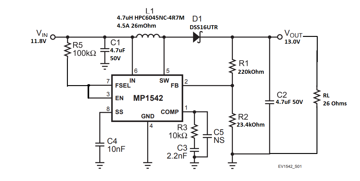
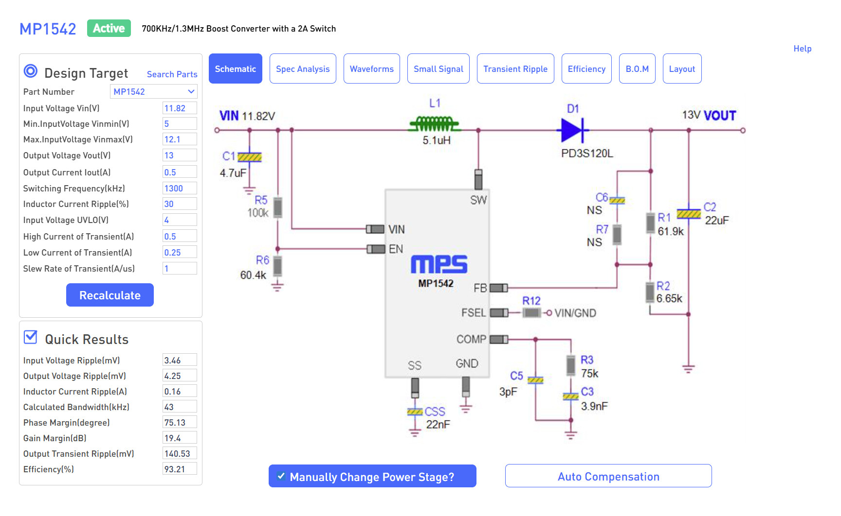
Hi Adhish, I tried the component network values recommended in the first screen capture (5.1uH, 22uF Cout, 75kOhm/3.9nF COMP), and the control loop was now unstable for any load current when input voltage was above 11.3V: and output voltage and COMP both exhibited sinusoidal oscillations. This is much worse than the problem I originally had, where the output was clean for most input voltages and load currents, and only exhibited operating frequency jump issues at particular light load operating points.

I think it’s clear that this isn’t dynamic instability (see additional work below). Would it be possible to get some feedback from MPS Design Engineering team on this issue? Is it possible that the part just isn’t appropriate for use at low switch duty cycles (10%)/low boost ratios(Vout/Vin=1.1), in a way that isn’t captured by either the datasheet or the Designer tool? Would the design team have any further recommendation for how to make the part transition in and out of light load reduced frequency operation at these low boost ratios without hysteresis-driven operating frequency oscillation?

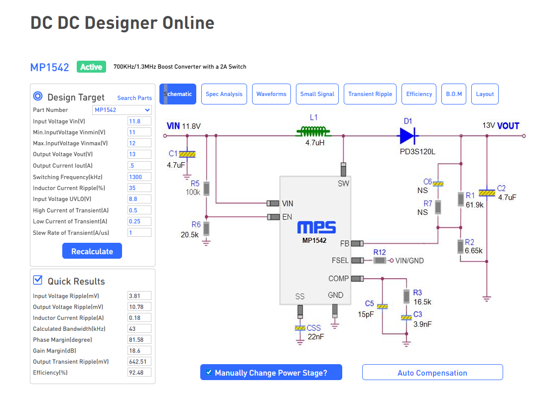
Some further work: by changing the Designer tool ripple allowance from the default of 30% to 35% the Designer now recommends a 4.7uH inductor. The app note says ripple up to 40% is typical (“Inductor Selection”, page 4) so 35% should be fine. I can also change the modeled output capacitor manually to 4.7uH to be in line with the datasheet table, and use Designer “Auto Compensation”, and I get phase margin of 81 deg and gain margin of 18dB with a recommended 16.5k/3.9nF COMP pin network. All indications are that this should be a stable operating point.

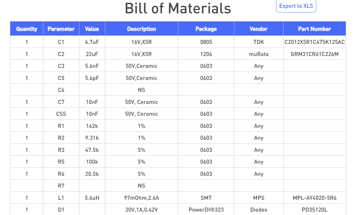
Placing 4.7uH, 4.7uF Cout, 16.5k/3.9nF COMP in the actual circuit results in clean operation for most load currents and most input voltages just as before, but still exhibits operating frequency jumps and triangular output ripple at specific low load current operating points, just as with the original 10k/2.2nF COMP parts.

So we’re now exactly following a set of Designer tool recommendations and have stable control loop operation, but this didn’t fix the issue. We’re still left with the original issue: the loop is stable, but at some particular light loads and input voltages, the part repeatedly jumps frequency, causing output ripple. At currents either above or below these points, and at input voltages above or below these points, the part’s output is stable and clean.

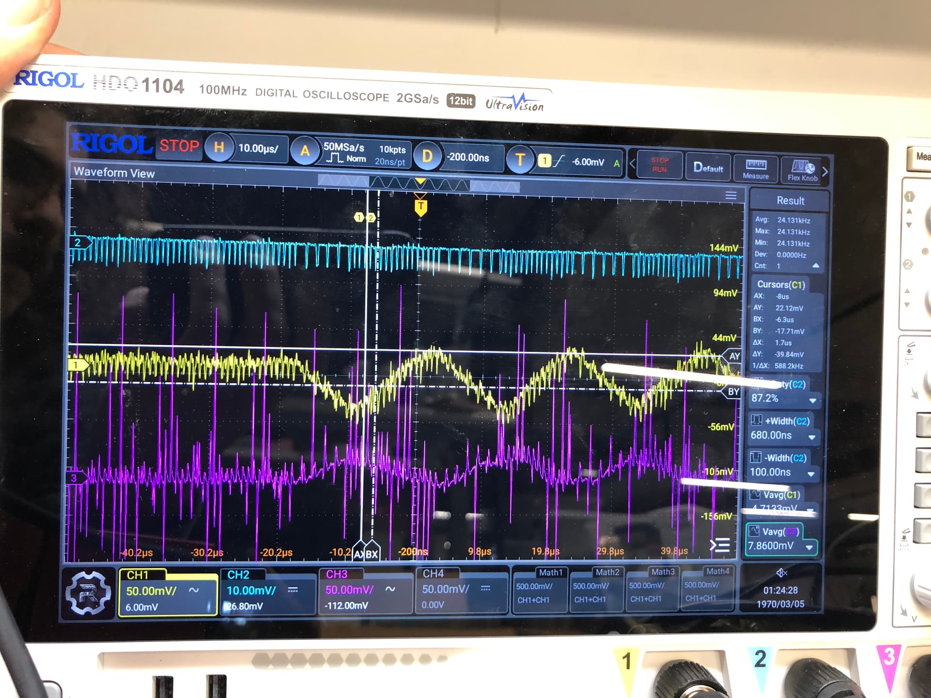
How can I say the loop is dynamically stable if there is an output ripple? I’ll include the following scope shot. This I think proves that what we’re seeing is not control loop instability related to the COMP pin network frequency response, but is caused by mode jumping between light load reduced frequency operating modes. I have finely adjusted the operating point (11.833Vin, 13Vout/0.35A resistive load) to the edge of a problem region so that the part jumps in and out of misbehavior randomly on it’s own, so we can see it starting to misbehave. This is with 4.7uF Cout, 16kOhm/3.9nF COMP. I can also get this to happen with all otherwise stable COMP/Cout values tested (22uF Cout, 5.1uH, 10k/2.2nF COMP; also 4.7uF Cout, 4.7uH, 10k/2.2nF COMP) by fine-tuning to slightly different input V and load I.

We have output voltage (yellow, AC coupled), switched node (blue, stray voltage pickup from a nearby probe) and COMP pin voltage (purple, AC coupled, sorry for the poor COMP probe grounding). The COMP pin DC voltage is 0.794V.

The feature I want to point out here is that COMP is perfectly flat aside from the probe grounding related spikes, and then the first thing that happens is that the switching frequency changes, and then the output voltage responds, and then finally the comp pin of course reflects the output via the feedback network. I think this shows that the output ripple and frequency variation is not caused by the comp network producing dynamic instability, but by the part transitioning between different light load reduced operating frequency modes back and forth, in a relaxation oscillation manner rather than in a dynamically unstable manner.

I’ll note that this happens regardless of whether I’m probing the COMP node or not, so this isn’t related to probe related noise injection (I am aware that the probe is definitely injecting some noise in the configuration shown above!).

Additionally the oscillation is triangular and begins instantly, and is not sinusoidal. This is indicative of an intentional operating frequency mode change due to hysteresis operating on some control variable (probably COMP pin voltage). This is not characteristic of dynamic instability, which would exhibit complex right half plane pole pair behavior (sinusoidal oscillation with exponential amplitude growth).

Anyway, thanks for your continued support on this, hoping we can figure out what’s going on here.

Hi Adhish,

I haven’t heard any response to my latest message, any update on this issue?

Thanks,

Ian

This topic was automatically closed 90 days after the last reply. New replies are no longer allowed.