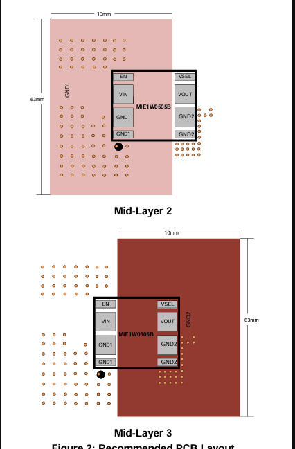
It is not recommended to have both GND planes of any isolated DC/DC system on the same layer.
Having these layers on the same layer even with clearance considerations would risk ground looping, possible radiation and conduction of noise, and in some cases can even risk isolation between your primary and secondary sides.
I would stick to the layout guidelines on this one.
As for the recommendations on Y-Caps, I would say anywhere between 4.7nF and 0.1uF would be suitable here.
Smaller values are better at minimizing leakage currents at the cost of less effective filtering.
Conversely, higher values will have a higher leakage at the benefit of providing better noise suppression and filtering capabilities.
Also remember to choose a Y-Cap that has a voltage rating higher than the max voltage that can be experienced in application to be safe. This includes potential unwarranted surge voltages.
The IC is on a 4 layer board that’s SIGNAL GND POWER SIGNAL. Separate layers would mean one of the ground planes goes in a power plane. Was just wondering if there were any risks associated with that as compared to putting them on the same layer with clearances