I need the correct I2C sequence for changing the output voltage and the current limit of a mEZDPD3603A / DIY8883 device. Can anybody help me?
1 Like
Hello Peter,
Thank you for utilizing the MPS Technical Forum.
For altering the output voltage using I2C:
→ you must adjust the internal Vref and the output feedback divider ratio. (Page 20 of DIY8883 datasheet)
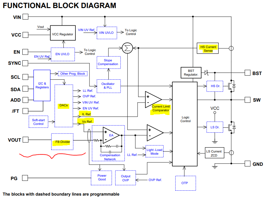
Please refer to the block diagram on understanding the interconnects within the part.
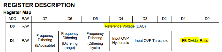
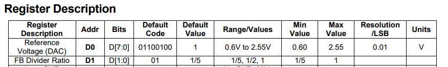
Register information for Vref and Voltage FB divider ratio.
For setting Current limits - please take note of hiccup default and SCP along with pk current limit and valley current limit adjustment. (Page 19 of Datasheet)
I will paste a capture of the register address for i2c sequencing.

Kind Regards,
Nouman
Thanks a lot for this information, but I already read the datasheet. When I change D0 and D1 as described, the output voltage turns to 0,5V no matter what I write to D0 or/and D1. What I need is the correct I2C sequence. In another thread I read that before writing the MTP has to be read, but no description how?
Hi Peter,
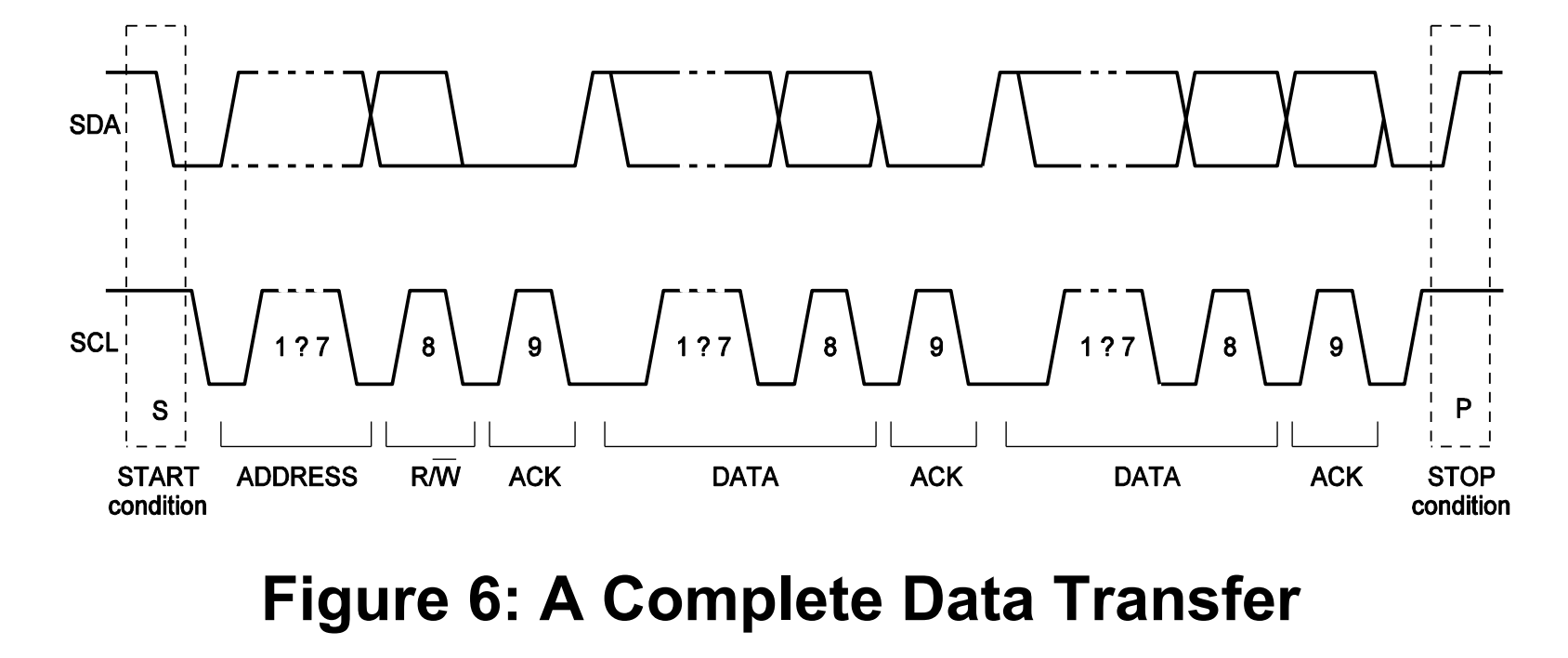
Can you please confirm if your SDA/SCL waveforms correspond with data transfer waveforms provided in the datasheet? (DIY8883 - under data transfer)
You might have to possibly debug if there are inconsistencies. This will help me in understanding why its not working on your end and possible replicate the issue once I get the parts on hand.
In your first post, you noted the EVB of this part too. Are you using the GUI for the evaluation board as well?
Regards,
Nouman
Hi Nouman,
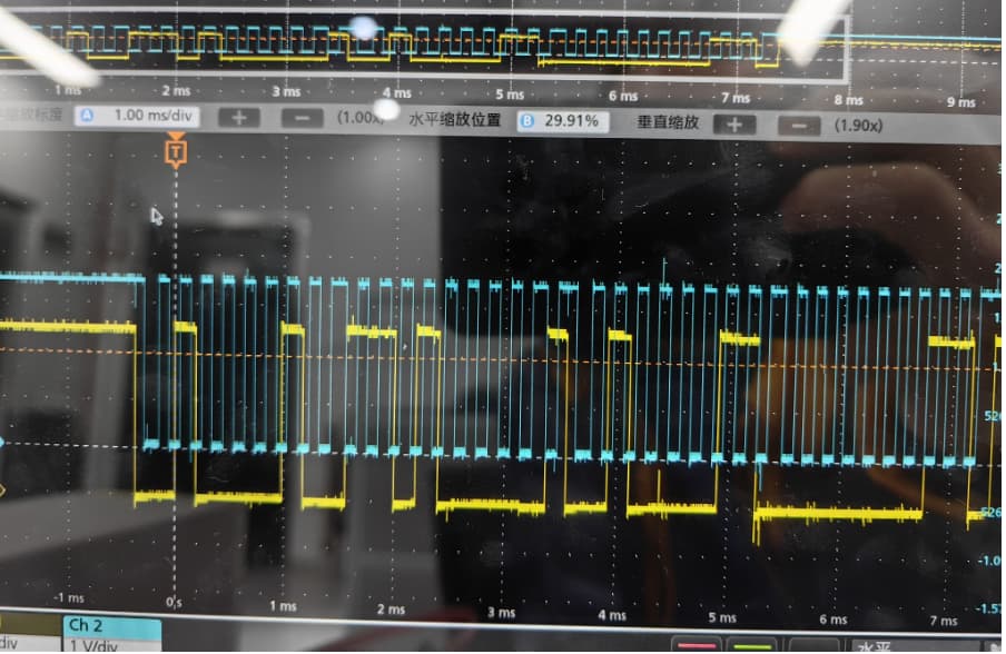
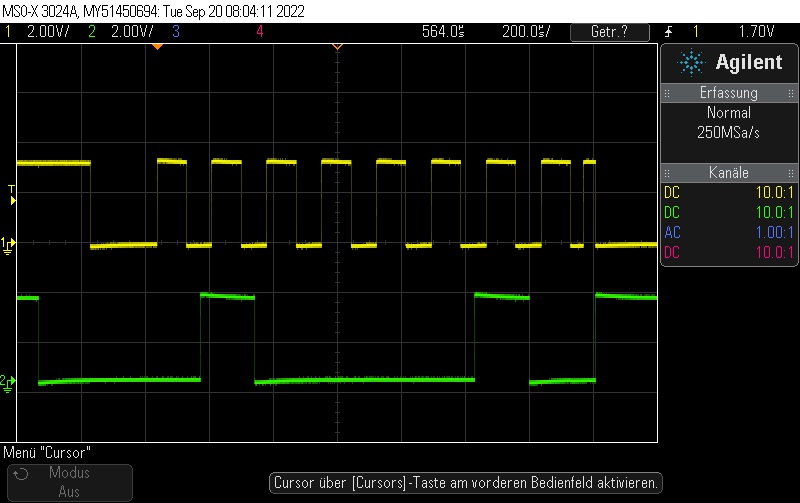
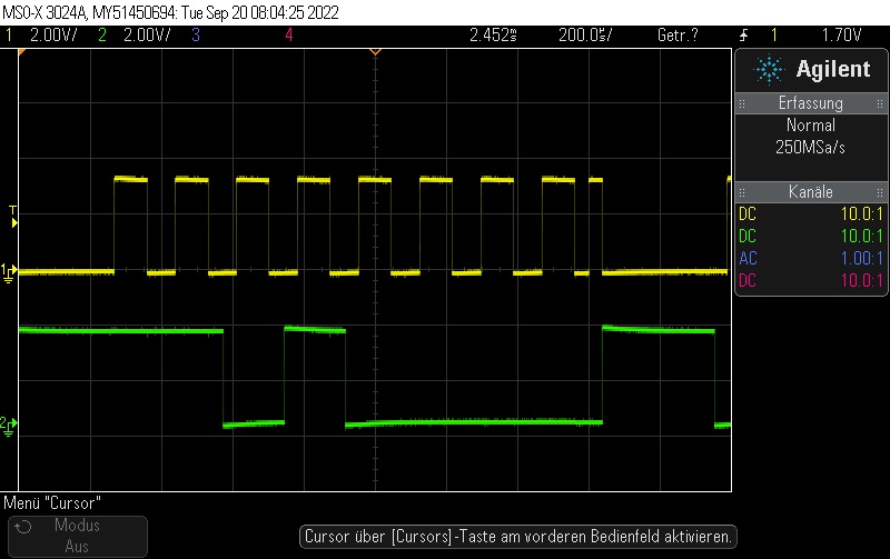
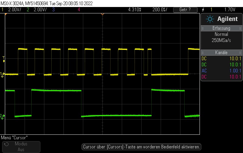
yes today I receive my evaluation board, but with this I can only program all the data , not a single register. So here are my oscilloscope screenshots of a write to 0xD0, value = 0x70. the first picture show the 3 Byte telegram the next pictures the single bytes. All the bytes get acknowledged by the DIY8883 but after this telegram the output voltage goes from 5V to 0V
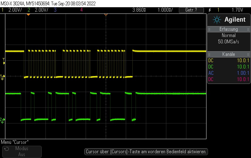
What I found out with the eval board is, that the read sequence is totaly different from the datasheet, it’s a 4 Byte telegram with a second start condition after the first two bytes. Nothing like this is written in the datasheet.
Best regards, Peter
Hi Peter,
I am looking into this and will get back to you with an answer. I am also having the part delivered so I can debug along with you.
If this is urgent for business purposes, then please reach out to MPSnow link below for us to delve further and provide technical support.
Kind Regards,
Nouman
Is there maybe any progress in this case? I see the same behavior.
What I learned tinkering with the module mEZDPD3603A-0001:
only addresses D0…DF are readable - writable (have ACK), but the write has no effect, except:
only the D0 address has any effect; if the LSB is 0 then the module stops. It can be written back to 1 or pull down the EN pin, and then it works again, so this is an enable bit. This bit can also read back as 0/1.
All other addresses read 0, except the ones not defined in the datasheet. All other writes has no effect. The output voltage doesn’t change regardless anything written anywhere.
I do not have the programmer to debug the communication.
There must be a proper way to access the registers, or at least change the output voltage.
Thanks,