I have a question regarding the ground connections in the gate driver component (we discussed this topic in the past).
I have 3 power stages on my board as shown in the illustration below—this is one out of the 3 stages.
Do I need to make the ground connection between AGND and PGND on each of the drivers, and should the connection between the grounds be close to each of the gate drivers?
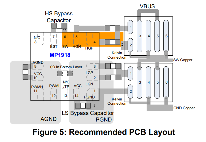
Thank you for posting to the MPS forum. You must connect AGND and PGND on each of the drivers for the best performance. The connection is recommended to be done with a 0 Ohm resistor placed between the two grounds on the bottom layer. An image from page 14 of the datasheet is attached below for your reference.
Hello, I am currently routing the MP1918 gate driver component along with the EPC2361 GaN FET, and I want to follow your recommendations for the gate driver layout precisely. Could you please provide a practical, step-by-step explanation for the following instructions: Divide the pins of the MP1918 into three blocks according to their functions. a. PWMH/L and VCC (pin 10) refer to the AGND. How should I handle this in the layout regarding the relation between PWMH/L and AGND? Does it mean that the AGND trace/plane should be routed very close to PWMH/L, and that the VCC (pin 10) connection should be placed close to AGND? b. LGP/N and VCC (pin 14) refer to the PGND. In this section as well, how should I practically implement the connection/routing for LGP/N and VCC (pin 14)? c. HGP/N and BST refer to the SW. Also in this section, how should I route and place these components practically? In addition, regarding the instruction: ‘Place a 0Ω resistor between AGND and PGND in the bottom layer’ — how should I implement this in practice? Since I am using an 8-layer board, should I connect the grounds on layer 8? And should it be done using a single plane?