Hello,
I’m working in a new design based on your MP4315 DCDC converter.
By one hand, I need to obtain 29V output from 32V input, nominal output current of 2A and maximum of 4A. According your online simulator it should run fine. It this device suitable for the commented use?
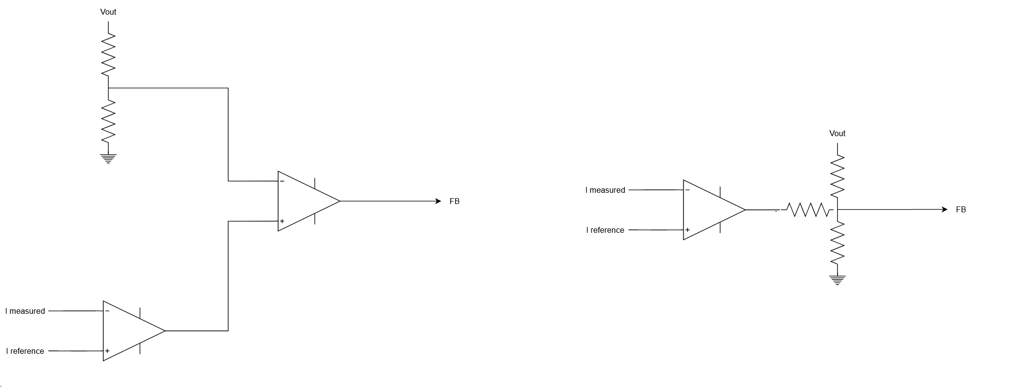
By the other hand, and this is my main doubt, I need to include CC/CV control with dynamic current reference. Do you have any reference guide to do it? These are two basic schemes of the circuit I have designed. If the main idea is to maintain 0.815V in the FB point, can the MP4315 support this fucntionality?
Thanks in advance. Best regards.
Miguel
Internet rando here, the other option is to play with the SS pin which per the block diagram is a separate input to the error amplifier equivalent to the FB input. So a current amplifer referenced to 1.6V or something like that whose output drives down as the current goes up and is 815mV at the desired charge current. Just a thought
Thanks @jshannon, I will try both options. I tested the first of them with good results in others converters at lower output voltage.
Regarding to the input/output voltage, what is the maximum duty cycle limit for the MP4315?
Thanks!
There is no way to tell from the datasheet. I would be looking at minimum off time and the frequency. Typically the min off time is 80 nsec if the switching period is 2usec then you could get a DC of 96% and the part should work. Sadly there is no spec for the maximum minimum off time so you have to take some kind of leap of faith that it isn’t too bad.
If for arguments sake you guess the worst case is 2x the typ, 160nsec that gives a 92% DC at 500khz and it would still work.
I would look for a demo board. So looks like DC is frequency dependent go slower if you need more DC.
On an encouraging note the datasheet shows scope shots of “low dropout mode” so they do kinda say it can operate well in that regime.
Dear jshannon,
I’ve tested the solution with the MP4315 working with the SS pin and it runs OK. It is not a perfect CC/CV regulator, but it seems good for our application.
Thanks for your support.
Hello jshannon,
I’m finishing the charger design and I’m working on the fine tuning, but unfortunately some parts have broken and I can not identify the cause.
Sometimes the IC input suddenly shortcircuit and it is not recoverable. After remove the IC the GND, Vin, SW, enable appears shorted internaly.
Do you know any general cause to obtain this result?
Thanks.
Hmm some chips have problems with prebiased outputs. As the chip is going through its softstart ramp and for instance is attempting to control a 4V battery to 1V, bad stuff can happen. In that case power will flow out of the battery to the input and boost the input voltage up perhaps until failure. You have to solder in another chip and start monitoring voltages and currents. I would look at the switching inductor current the battery voltage and perhaps the input voltage to try to get a sense of what is going on.
I think you want to use the AAM which lets the bottom fet emulate a diode, this should mitigate the problem of power flowing out of the battery back to the input and possibly blowing everything up.
Thanks @jshannon, I’m using a schottky diode in the converter output to avoid reverse currents and I’m now using AAM. I’m going to investigate it and I will let you know. Thanks for the advice.