Buck Boost Design

Hi,
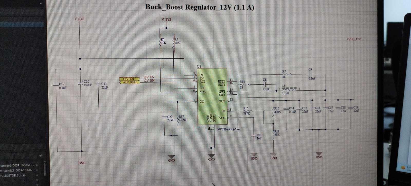
I would like to know whether the design given below can be used to for a Buck Boost that has input range from 10.8-16.8V and Output 12V. Output current is 0.5A.
This is the application circuit that I got from datasheet of MP28167GQ-A-Z.

Could you please clear a few more questions regarding the design?

  1. I would like to know the equation for calculating the inductor value for Buck Boost converter.
  2. Could you please specify the VIH and VIL for the Enable pin?
  3. Is the ALT (Alert) pin open drain? If not so then what would be the voltage in that pin?
  4. Is I2C mandatory for this design?
  5. If I2C is not used in the design, the is it in PFM of PWM mode?

Hello,

Apologies for the delay in response.

  1. Calculation and recommendation of the inductor should be specified on pg28 of the datasheet.
  2. The enable rising threshold is specified towards the top of the EC table on pg 7.
  3. I believe it is open drain. Referring to the typical application circuit, it is pulled up to VCC with pull up resistor.
  4. I2C is used to configure parameters different to the default settings. Note: If I2C is not used, make sure to follow the datasheet regarding the I2C lines. For example, SCL and SDA should be pulled up to VCC if not used.
  5. The default mode is PWM mode under light load conditions.

Best Regards,
Yu